121 results on '"Antonio Tejeda"'
Number of results to display per page
Search Results
2. Effective determination of surface potential landscapes from metal-organic nanoporous network overlayers
- Author
-
Ignacio Piquero-Zulaica, Zakaria M Abd El-Fattah, Olha Popova, Shigeki Kawai, Sylwia Nowakowska, Manfred Matena, Mihaela Enache, Meike Stöhr, Antonio Tejeda, Amina Taleb, Ernst Meyer, J Enrique Ortega, Lutz H Gade, Thomas A Jung, and Jorge Lobo-Checa
- Subjects
metal-organic nanoporous networks ,electron confinement ,electronic band structure ,modelization ,Science ,Physics ,QC1-999 - Abstract
Determining the scattering potential landscape for two-dimensional superlattices provides key insight into fundamental quantum electron phenomena. Theoretical and semiempirical methods have been extensively used to simulate confinement effects of the two-dimensional electron gas (2DEG) on superlattices with a single scatterer in the form of vicinal surfaces and dislocation networks or isolated structures such as quantum corrals and vacancy islands. However, the complexity of the problem increases when the building blocks (or scatterers) are heterogeneous, as in metal-organic nanoporous networks (MONNs), since additional potentials may come into play. Therefore, the parametrization of the surface potential landscape is often inaccurate, leading to incorrect scattering potentials. Here, we address this issue with a combination of scanning tunneling microscopy/spectroscopy, angle resolved photoemission spectroscopy and Kelvin probe force microscopy measurements together with electron plane-wave expansion simulations on a MONN grown on Cu(111). This experimental-theory approach, enables us to capture the 2DEG response to the intricate scattering potential landscape, and reveals systematic modeling procedures. Starting from a realistic geometry of the system, we determine the repulsive scattering potentials for both molecules and coordinated metal adatoms, the latter contradicting the established simulation framework. Moreover, we reveal local asymmetries and subtle renormalization effects of the 2DEG that relate to the interaction of the MONN and the underlying substrate.
- Published
- 2019
- Full Text
- View/download PDF
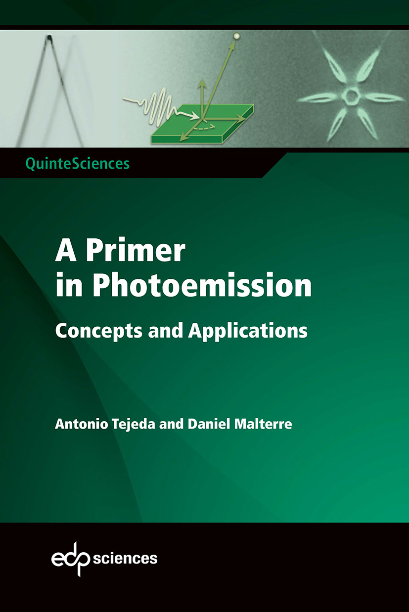
3. A Primer in Photoemission: Concepts and Applications
- Author
-
Antonio Tejeda, Daniel Malterre and Antonio Tejeda, Daniel Malterre
- Published
- 2019
4. Rates Changes and Earnings Management in the Domestic Energy Suppliers/Alteracoes de Taxas e Gestao de Resultados nas Distribuidoras de Energia Eletrica Domestica
- Author
-
Cruz, Jonas da Costa and Almonte, Jose Antonio Tejeda
- Published
- 2019
- Full Text
- View/download PDF
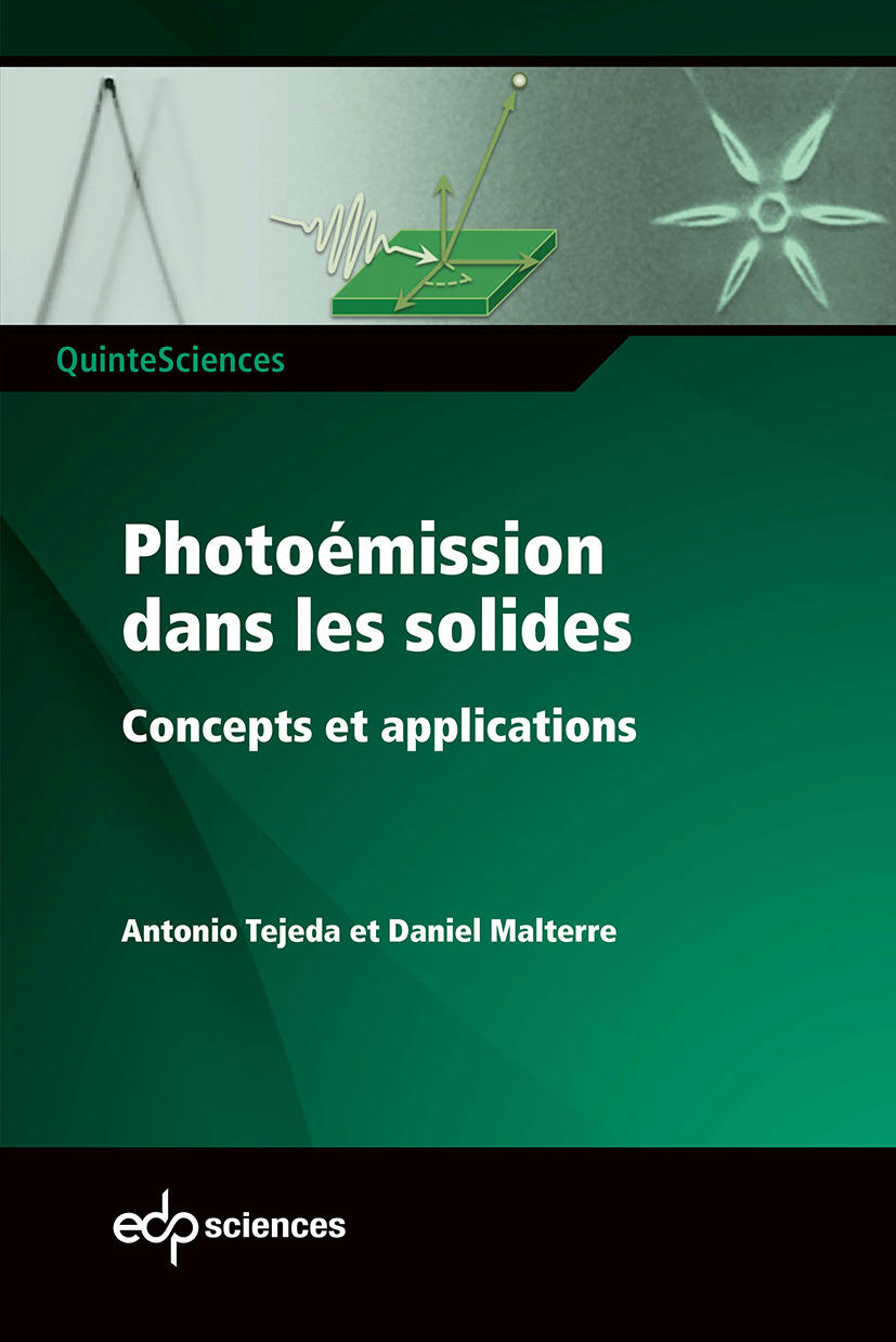
5. Photoémission dans les solides: Concepts et applications
- Author
-
Antonio Tejeda, Daniel Malterre and Antonio Tejeda, Daniel Malterre
- Published
- 2016
6. Epigraphene: the first viable platform for seamless zero-mode graphene nanoelectronics
- Author
-
Vladimir Prudkovskiy, Yiran Hu, Yue Hu, Kaimin Zhang, Peixuan Ji, Grant Nunn, Jian Zhao, Chengqian Shi, Antonio Tejeda, David Wander, Alessandro de Cecco, Clemens Winkelmann, Yuxuan Jiang, Tianhao Zhao, Katsunori Wakabayashi, Zhigang Jiang, Lei Ma, Claire Berger, and Walt de Heer
- Abstract
A graphene nanoelectronics platform -envisioned as scalable seamlessly integrated graphene nanoscale devices -has failed to materialize due to pervasive edge disorder caused by lithographic processes that diminish the mobility and destroy the edge state in exfoliated graphene nanoribbons. Here we demonstrate, for the first time, graphene edge state transport in conventionally patterned graphene ribbon networks produced on graphene that is epitaxially grown on non-polar faces of electronics grade silicon carbide wafers (epigraphene). The epigraphene edge state is extremely robust to lithography processing, as the graphene edge atoms bind to the SiC substrate. The protected edge state has a mean free path that is greater than 50 microns, 5000 times greater than the bulk states. It involves a non-degenerate, spin polarized, zero-energy electronic band that does not produce a Hall voltage. In seamless integrated structures, the edge state forms a zero-energy one-dimensional ballistic network with essentially dissipationless nodes at ribbon-ribbon junctions. Its novel properties point to an unconventional charge carrier that is half-electron and half-hole. Seamless integrated graphene edge state device structures that are phase coherent at low temperatures offer a variety of switching possibilities. This makes epigraphene the only technologically viable graphene nanoelectronics platform that has the potential to succeed silicon nanoelectronics.
- Published
- 2022
7. Dynamics of the Structural Modification of CH3NH3PbI3 Hybrid Perovskite upon Visible-Light Excitation
- Author
-
Abraham Campos-Contreras, Antonio Tejeda, Lipin Chen, Amelie Jarnac, Claire Laulhé, Min-I Lee, Emmanuelle Deleporte, Olivier Plantevin, David Le Bolloc'h, Vincent Jacques, and Gaelle Trippé-Allard
- Published
- 2022
8. A habilidade do gestor CFO e sua relação com a eficiência das empresas listadas na bolsa de valores brasileira
- Author
-
Andréia Hartwig, Jose Antonio Tejeda Almonte, and Taianan Alves Uzeda Luna
- Subjects
Materials Chemistry - Abstract
Este estudo analisou o efeito da capacidade gerencial do diretor financeiro (CFO) na qualidade dos resultados divulgados pelas firmas listadas na B3. Para obter a capacidade gerencial do CFO foi utilizada a abordagem de Demerjian et al. (2013), na qual se estima a eficiência total da empresa mediante um método de fronteira eficiente e o resíduo da equação é tomado para criação da medida. Foi utilizada a reapresentação dos resultados contábeis como proxy de qualidade de resultados da firma. Foi considerado como eficiência da firma a capacidade de agregar valor aos insumos adquiridos ou consumidos. A eficiência foi estimada através do método de Stochastic Production Frontier (SFA), mediante um fixed effects production frontier model. Para verificar se a parcela de eficiência da firma atribuível a capacidade do CFO e a sua equipe tem relação com a qualidade dos resultados foi estimado um modelo de regressão probit em painel mediante o generalized estimating equation (GEE) approach para descobrir o efeito médio na população da variável que representa a capacidade gerencial, Mhabil, em relação ao efeito específico individual. As evidências empíricas indicam que maior capacidade gerencial do CFO tem relação negativa com a probabilidade de reapresentação dos relatórios financeiros e, consequentemente, maior a qualidade dos resultados para as empresas. Os resultados indicam que a escolha do gestor CFO é importante para o mercado de capitais, demonstrando que CFOs mais capazes implicam em menores chances de reapresentação dos resultados financeiros. Para a análise foram utilizadas informações anuais das empresas brasileiras listadas na B3 no período de 2010 a 2017.
- Published
- 2020
9. Photoemission signature of momentum-dependent hybridization in CeCoIn5
- Author
-
Antonio Tejeda, Dariusz Kaczorowski, Jozef Spałek, K. Kissner, François Bertran, Julien E. Rault, Jan Minár, Friedrich Reinert, Laurent Nicolaï, Ł. Walczak, Maciej Fidrysiak, Dominik Legut, Marcin Rosmus, P. Starowicz, R. Kurleto, Daniel Gnida, and Andrzej P. Kądzielawa
- Subjects
Physics ,Strongly Correlated Electrons (cond-mat.str-el) ,Condensed matter physics ,Photoemission spectroscopy ,f electrons, photoemission, resonant ARPES ,FOS: Physical sciences ,Fermi surface ,Fermi energy ,Angle-resolved photoemission spectroscopy ,Photon energy ,Heavy fermion superconductor ,Brillouin zone ,Condensed Matter - Strongly Correlated Electrons ,Tight Binding model ,Wave vector ,hybridization ,multiple scattering KKR - Abstract
Hybridization between $f$ electrons and conduction bands ($c$-$f$ hybridization) is a driving force for many unusual phenomena. To provide insight into it, systematic studies of CeCoIn$_5$ heavy fermion superconductor have been performed by angle-resolved photoemission spectroscopy (ARPES) in a large angular range at temperature of $T=6$ K. The used photon energy of 122 eV corresponds to Ce $4d$-$4f$ resonance. Calculations carried out with relativistic multiple scattering Korringa-Kohn-Rostoker method and one-step model of photoemission yielded realistic simulation of the ARPES spectra indicating that Ce-In surface termination prevails. Surface states, which have been identified in the calculations, contribute significantly to the spectra. Effects of the hybridization strongly depend on wave vector. They include a dispersion of heavy electrons and bands gaining $f$-electron character when approaching Fermi energy. We have also observed a considerable variation of $f$-electron spectral weight at $E_F$, which is normally determined by both matrix element effects and wave vector dependent $c$-$f$ hybridization. Fermi surface scans covering a few Brillouin zones revealed large matrix element effects. A symmetrization of experimental Fermi surface, which reduces matrix element contribution, yielded a specific variation of $4f$-electron enhanced spectral intensity at $E_F$ around $\bar{\Gamma}$ and $\bar{M}$ points. Tight-binding approximation calculations for Ce-In plane provided the same universal distribution of $4f$-electron density for a range of values of the parameters used in the model., Comment: 15 pages, 9 figures
- Published
- 2021
10. Dissipationless zero energy epigraphene edge state for nanoelectronics
- Author
-
Jian Zhao, Clemens Winkelmann, Kaimin Zhang, Vladimir Prudkovskiy, Katsunori Wakabayashi, Zhigang Jiang, Chengqian Shi, Antonio Tejeda, Tianhao Zhao, Yiran Hu, Walt A. de Heer, Peixuan Ji, David Wander, Alessandro de Cecco, Yue Hu, Lei Ma, Yuxuan Jiang, Grant Nunn, Claire Berger, Georgia Tech Lorraine [Metz], Université de Franche-Comté (UFC), Université Bourgogne Franche-Comté [COMUE] (UBFC)-Université Bourgogne Franche-Comté [COMUE] (UBFC)-Ecole Supérieure d'Electricité - SUPELEC (FRANCE)-Georgia Institute of Technology [Atlanta]-CentraleSupélec-Ecole Nationale Supérieure des Arts et Metiers Metz-Centre National de la Recherche Scientifique (CNRS), School of Electrical and Computer Engineering - Georgia Insitute of Technology (ECE GeorgiaTech), and Georgia Institute of Technology [Atlanta]
- Subjects
[SPI]Engineering Sciences [physics] ,Materials science ,Condensed matter physics ,Nanoelectronics ,0103 physical sciences ,Zero-point energy ,02 engineering and technology ,State (functional analysis) ,Edge (geometry) ,021001 nanoscience & nanotechnology ,010306 general physics ,0210 nano-technology ,01 natural sciences - Abstract
The graphene edge state is essential for graphene electronics and fundamental in graphene theory, however it is not observed in deposited graphene. Here we report the discovery of the epigraphene edge state (EGES) in conventionally patterned epigraphene using plasma-based lithography that stabilizes and passivates the edges probably by fusing the graphene edges to the non-polar silicon carbide substrate, as expected. Transport involves a single, essentially dissipationless conductance channel at zero energy up to room temperature. The Fermi level is pinned at zero energy. The EGES does not generate a Hall voltage and the usual quantum Hall effect is observed only after subtraction of the EGES current. EGES transport is highly protected and apparently mediated by an unconventional zero-energy fermion that is half electron and half hole. Interconnected networks involving only the EGES can be patterned, opening the door to a new graphene nanoelectronics paradigm that is relevant for quantum computing.
- Published
- 2021
11. Renormalization of the valence and conduction bands of (C6H5C2H4NH3)(2)PbI4 hybrid perovskite
- Author
-
A Barragán, J.-M. Themlin, Hela Mrezguia, Maya N. Nair, J. Minár, Saleem Ayaz Khan, L. Giovanelli, Gaëlle Trippé-Allard, Antonio Tejeda, Hamza Khelidj, Ferdinand Lédée, Amina Taleb-Ibrahimi, Min-I Lee, Emmanuelle Deleporte, Younal Ksari, Laboratoire de Physique des Solides (LPS), Université Paris-Saclay-Centre National de la Recherche Scientifique (CNRS), University of West Bohemia [Plzeň ], Institut des Matériaux, de Microélectronique et des Nanosciences de Provence (IM2NP), Université de Toulon (UTLN)-Centre National de la Recherche Scientifique (CNRS)-Aix Marseille Université (AMU), Synchrotron SOLEIL (SSOLEIL), Centre National de la Recherche Scientifique (CNRS), Laboratoire Lumière, Matière et Interfaces (LuMIn), CentraleSupélec-Université Paris-Saclay-Centre National de la Recherche Scientifique (CNRS)-Ecole Normale Supérieure Paris-Saclay (ENS Paris Saclay), and Aix Marseille Université (AMU)-Université de Toulon (UTLN)-Centre National de la Recherche Scientifique (CNRS)
- Subjects
spin–orbit coupling ,(C6H5C2H4NH3)2PbI4 ,Materials science ,Acoustics and Ultrasonics ,Photoemission spectroscopy ,Inverse photoemission spectroscopy ,Angle-resolved photoemission spectroscopy ,02 engineering and technology ,Electronic structure ,7. Clean energy ,01 natural sciences ,Renormalization ,inverse photoemission spectroscopy ,Condensed Matter::Materials Science ,Photovoltaics ,Condensed Matter::Superconductivity ,2D hybrid organic-inorganic perovskites ,0103 physical sciences ,angle-resolved photoemission spectroscopy ,phenylethylammonium lead iodine ,010306 general physics ,Perovskite (structure) ,Valence (chemistry) ,Condensed matter physics ,business.industry ,k-resolved band structures ,021001 nanoscience & nanotechnology ,Condensed Matter Physics ,Surfaces, Coatings and Films ,Electronic, Optical and Magnetic Materials ,[PHYS.COND.CM-MS]Physics [physics]/Condensed Matter [cond-mat]/Materials Science [cond-mat.mtrl-sci] ,Condensed Matter::Strongly Correlated Electrons ,0210 nano-technology ,business - Abstract
International audience; Quasi two-dimensional hybrid organic-inorganic perovskites (HOIPs) have been rediscovered recently for photovoltaics due to a higher stability than other HOIPs. We focus here on the electronic structure of the 2D perovskite (C6H5C2H4NH3)2PbI4. We perform an experimental k-resolved determination of the valence and conduction bands by angle-resolved photoemission spectroscopy (ARPES) and inverse photoemission spectroscopy (IPES). The experimental and theoretical dispersions are compared. The valence band width is in agreement with that of renormalized theoretical bands, while no significative renormalization is observed for the conduction band. The effect of the spin-orbit coupling in the conduction band is also experimentally observed.
- Published
- 2021
12. Doping Graphene with Substitutional Mn
- Author
-
Stefan De Gendt, Antonio Tejeda, L. M. C. Pereira, Maya N. Nair, Renan Villarreal, Hans Hofsäss, Luca Petaccia, Simona Achilli, Guido Fratesi, Giovanni Di Santo, Harsh Bana, Manuel Auge, Ken Verguts, Steven Brems, Pin-Cheng Lin, Steven De Feyter, Laboratoire de Physique des Solides (LPS), and Université Paris-Saclay-Centre National de la Recherche Scientifique (CNRS)
- Subjects
Materials science ,Magnetism ,General Physics and Astronomy ,doping ,02 engineering and technology ,Electronic structure ,010402 general chemistry ,01 natural sciences ,law.invention ,law ,Vacancy defect ,Physics::Atomic and Molecular Clusters ,ion implantation ,General Materials Science ,Electronic band structure ,Superstructure ,Condensed matter physics ,Graphene ,graphene ,Doping ,General Engineering ,electronic structure ,021001 nanoscience & nanotechnology ,0104 chemical sciences ,Ion implantation ,magnetism ,manganese ,[PHYS.COND.CM-MS]Physics [physics]/Condensed Matter [cond-mat]/Materials Science [cond-mat.mtrl-sci] ,0210 nano-technology - Abstract
We report the incorporation of substitutional Mn atoms in high-quality, epitaxial graphene on Cu(111), using ultralow-energy ion implantation. We characterize in detail the atomic structure of substitutional Mn in a single carbon vacancy and quantify its concentration. In particular, we are able to determine the position of substitutional Mn atoms with respect to the Moiré superstructure (i.e., local graphene-Cu stacking symmetry) and to the carbon sublattice; in the out-of-plane direction, substitutional Mn atoms are found to be slightly displaced toward the Cu surface, that is, effectively underneath the graphene layer. Regarding electronic properties, we show that graphene doped with substitutional Mn to a concentration of the order of 0.04%, with negligible structural disorder (other than the Mn substitution), retains the Dirac-like band structure of pristine graphene on Cu(111), making it an ideal system in which to study the interplay between local magnetic moments and Dirac electrons. Our work also establishes that ultralow-energy ion implantation is suited for substitutional magnetic doping of graphene. Given the flexibility, reproducibility, and scalability inherent to ion implantation, our work creates numerous opportunities for research on magnetic functionalization of graphene and other two-dimensional materials. PMID: 33596385 ispartof: ACS NANO vol:15 issue:3 pages:5449-5458 ispartof: location:United States status: published
- Published
- 2021
- Full Text
- View/download PDF
13. Photoémission dans les solides
- Author
-
Daniel Malterre and Antonio Tejeda
- Published
- 2020
14. A Primer in Photoemission
- Author
-
Antonio Tejeda and Daniel Malterre
- Published
- 2020
15. Correction to Doping Graphene with Substitutional Mn
- Author
-
Pin-Cheng Lin, Renan Villarreal, Simona Achilli, Harsh Bana, Maya N. Nair, Antonio Tejeda, Ken Verguts, Stefan De Gendt, Manuel Auge, Hans Hofsäss, Steven De Feyter, Giovanni Di Santo, Luca Petaccia, Steven Brems, Guido Fratesi, and Lino M. C. Pereira
- Subjects
General Engineering ,General Physics and Astronomy ,General Materials Science - Published
- 2022
16. On the energy resolution of a GaAs-based electron source for spin-resolved inverse photoemission
- Author
-
Abraham Federico Campos, Thomas Duden, and Antonio Tejeda
- Abstract
The spin resolution in inverse photoemission spectroscopy is achieved by injecting spin-polarized electrons, usually produced by GaAs-based cold cathodes that replace hot-filament electron guns of spin-integrated setups. The overall energy resolution of the system can be enhanced by adjusting either the optical bandpass of the photon detector or the energy distribution of the electron beam. Here we discuss the influence of the photocurrent and the photocathode temperature on the energy broadening of the electron beam through the inverse photoemission spectra of the spin-splitted Shockley surface state of Au(111). First, we find that cooling down the GaAs photocathode to 77 K increases the band gap and reduces the number of allowed vertical transitions, monochromatizing the electron beam with an enhancement of about 30 meV for the energy resolution. Second, we observe a correlation between the generated photocurrent at the electron source, and the space-charge effects at the sample as a reduction of lifetime and spin asymmetry of a polarized bulk state. These observations allow defining a threshold of current density for the optimum acquisition in the measurements of spin-resolved inverse photoemission in Au.
- Published
- 2022
17. Hybrid perovskites for photovoltaics and optoelectronics
- Author
-
Wallace C. H. Choy, Emmanuelle Deleporte, Michael Grätzel, Antonio Tejeda, Laboratoire de Physique des Solides (LPS), Université Paris-Saclay-Centre National de la Recherche Scientifique (CNRS), The University of Hong Kong (HKU), Laboratoire Lumière, Matière et Interfaces (LuMIn), CentraleSupélec-Université Paris-Saclay-Centre National de la Recherche Scientifique (CNRS)-Ecole Normale Supérieure Paris-Saclay (ENS Paris Saclay), Nano Optique et Spectroscopy (NOOS), CentraleSupélec-Université Paris-Saclay-Centre National de la Recherche Scientifique (CNRS)-Ecole Normale Supérieure Paris-Saclay (ENS Paris Saclay)-CentraleSupélec-Université Paris-Saclay-Centre National de la Recherche Scientifique (CNRS)-Ecole Normale Supérieure Paris-Saclay (ENS Paris Saclay), and Ecole Polytechnique Fédérale de Lausanne (EPFL)
- Subjects
Materials science ,Acoustics and Ultrasonics ,business.industry ,Nanotechnology ,010402 general chemistry ,Condensed Matter Physics ,01 natural sciences ,0104 chemical sciences ,Surfaces, Coatings and Films ,Electronic, Optical and Magnetic Materials ,Photovoltaics ,[PHYS.COND.CM-MS]Physics [physics]/Condensed Matter [cond-mat]/Materials Science [cond-mat.mtrl-sci] ,business ,ComputingMilieux_MISCELLANEOUS - Abstract
International audience
- Published
- 2020
18. Growth, morphology and electronic properties of epitaxial graphene on vicinal Ir(332) surface
- Author
-
François Nicolas, Daniel Malterre, Antonio Tejeda, A. Taleb-Ibrahimi, Stefan Kubsky, Arlensiú Celis, Muriel Sicot, Maya N. Nair, Laboratoire de Physique des Solides (LPS), Université Paris-Saclay-Centre National de la Recherche Scientifique (CNRS), Synchrotron SOLEIL (SSOLEIL), Centre National de la Recherche Scientifique (CNRS), City University of New York [New York] (CUNY), Institut Jean Lamour (IJL), Université de Lorraine (UL)-Institut de Chimie du CNRS (INC)-Centre National de la Recherche Scientifique (CNRS), and Université de Lorraine (UL)-Centre National de la Recherche Scientifique (CNRS)
- Subjects
Materials science ,Band gap ,Photoemission spectroscopy ,Superlattice ,growth ,photoelectron spectroscopy ,Bioengineering ,Angle-resolved photoemission spectroscopy ,02 engineering and technology ,010402 general chemistry ,01 natural sciences ,law.invention ,law ,General Materials Science ,Electrical and Electronic Engineering ,Electronic band structure ,ComputingMilieux_MISCELLANEOUS ,Low-energy electron diffraction ,business.industry ,Graphene ,superperiodicity ,Mechanical Engineering ,General Chemistry ,021001 nanoscience & nanotechnology ,0104 chemical sciences ,bandgap ,Mechanics of Materials ,electronic properties ,[PHYS.COND.CM-MS]Physics [physics]/Condensed Matter [cond-mat]/Materials Science [cond-mat.mtrl-sci] ,Optoelectronics ,0210 nano-technology ,business ,Vicinal - Abstract
International audience; Superlattice induced minigaps in graphene band structure due to underlying one-dimensional nanostructuration has been demonstrated. A superperiodic potential can be introduced in graphene if the substrate is periodically structured. The successful preparation of a periodically nanostructured substrate in large scale can be obtained by carefully studying the electronic structure with a spatial averaging technique such as high-energy resolution photoemission. In this work, we present two different growth methods such as temperature programmed growth (TPG) and chemical vapor deposition (CVD) studied by scanning tunnelling microscopy (STM) and low energy electron diffraction (LEED). In both methods, we show that the original steps of Ir(332) have modified with (111) terraces and step bunching after graphene growth. Graphene grows continuously over the terrace and the step bunching areas. We observe that while TPG growth does not give rise to a well-defined surface periodicity required for opening a bandgap, the CVD growth does. By combining with angle-resolved photoemission spectroscopy (ARPES) measurements, we correlate the obtained spatial periodicity to observed band gap opening in graphene.
- Published
- 2020
19. Rates Changes and Earnings Management in the Domestic Energy Suppliers
- Author
-
Jonas da Costa Cruz and Jose Antonio Tejeda Almonte
- Subjects
Finance ,Distribuidoras de energia elétrica ,electric power distributors ,Periodic Tariff Readjustment ,Earning management ,Notice ,business.industry ,Accrual ,Tariff ,Sample (statistics) ,General Medicine ,Gerenciamento de resultados ,Earnings management ,Order (exchange) ,Revisão Tarifária Periódica ,Value (economics) ,Business ,Panel data - Abstract
Objective: To verify whether the concessionaires of electric energy adopt earnings management (EM) practices, before and after the Periodic Tariff Review (PTR), in order to obtain better rates and attract investors and/or pay bonuses to their managers.Method: The sample of this study contains all electric power utility companies of B3, covering the period of 2010-2016. We analyzed the impact of PTR using the panel data method.Originality/Relevance: It was analyzed whether the EM is related to PTR, since the interest of the consumer, the government and the investors is different of the concessionary´s interest with respect to the value of the tariff. Notice that investors can make better decisions on how and when to allocate their resources to a specific PTR event.Theoretical/Methodological Contributions: The findings indicate that in the years of tariff review, there is a greater generation of accruals and dimishments 2 years after the PTR. On the other hand, in EM (operational) the cyclical behavior is similar, but the PTR is negative in the year of the tariff review and positive two periods ahead.Social contributions to management: These results are understood as long as the concessionaires know that the result of the year of PTR will not influence the Regulatory Agency in the determination of the present revision and reverse them 2 periods ahead, in order to anticipate for the next PTR., Objetivo: Verificar se as empresas concessionárias de energia elétrica adotam práticas de gerenciamento de resultados (GR), em momentos anteriores e posteriores à Revisão Tarifária Periódica (RTP), a fim de obterem melhores tarifas, atraírem investidores e/ou pagar bonificações aos seus gestores.Método: A amostra de este estudo é composta por todas as empresas concessionárias de energia elétrica da B3, cobrindo o período 2010-2016. Analisamos o impacto da RTP mediante o método de dados em painel.Originalidade/Relevância: Analisou-se se o GR está relacionado à RTP, dado que o interesse do consumidor, do governo e dos investidores é diferente ao das empresas concessionárias no tocante ao valor da tarifa. Veja que os investidores podem tomar melhores decisões em como e quando alocar os seus recursos no evento específico da RTP.Resultados: Notamos que, na média, as empresas gerenciam os seus resultados para cima após a RTP e para baixo nos anos de tarifação.Contribuições Teóricas/Metodológicas: Os achados indicam que nos anos de revisão tarifária existe maior geração de accruals e diminuídos 2 anos após o RTP. Por outro lado, no GR (operacional) o comportamento cíclico é similar, mas a RTP é um fator negativo no ano da revisão tarifária e positivo dois períodos a frente.Contribuições sociais para a gestão: Estes resultados são compreendidos desde que as empresas concessionárias sabem que o resultado do ano da RTP não influenciará a agência reguladora na determinação da revisão presente e os revertem 2 períodos a frente, no intuito de se antecipar para a próxima RTP.
- Published
- 2019
20. An epitaxial graphene platform for zero-energy edge state nanoelectronics
- Author
-
Vladimir S. Prudkovskiy, Yiran Hu, Kaimin Zhang, Yue Hu, Peixuan Ji, Grant Nunn, Jian Zhao, Chenqian Shi, Antonio Tejeda, David Wander, Alessandro De Cecco, Clemens B. Winkelmann, Yuxuan Jiang, Tianhao Zhao, Katsunori Wakabayashi, Zhigang Jiang, Lei Ma, Claire Berger, Walt A. de Heer, Tianjin University (TJU), Georgia Institute of Technology [Atlanta], Laboratoire de Physique des Solides (LPS), Université Paris-Saclay-Centre National de la Recherche Scientifique (CNRS), Synchrotron SOLEIL (SSOLEIL), Centre National de la Recherche Scientifique (CNRS), Nano-Electronique Quantique et Spectroscopie (NEEL - QuNES), Institut Néel (NEEL), Centre National de la Recherche Scientifique (CNRS)-Université Grenoble Alpes (UGA)-Institut polytechnique de Grenoble - Grenoble Institute of Technology (Grenoble INP ), Université Grenoble Alpes (UGA)-Centre National de la Recherche Scientifique (CNRS)-Université Grenoble Alpes (UGA)-Institut polytechnique de Grenoble - Grenoble Institute of Technology (Grenoble INP ), Université Grenoble Alpes (UGA), National High Magnetic Field Laboratory (NHMFL), Florida State University [Tallahassee] (FSU), Kwansei Gakuin University, Circuits électroniques quantiques Alpes (NEEL - QuantECA), Georgia Institute of Technology [Lorraine, France], ANR-19-CE24-0025,BONNEG,Films bidimensionnels épitaxiés BN/epigraphène/SiC pour la nanoélectronique(2019), European Project: 696656,H2020,H2020-Adhoc-2014-20,GrapheneCore1(2016), and European Project: 785219,H2020,GrapheneCore2(2018)
- Subjects
Condensed Matter - Materials Science ,Multidisciplinary ,Condensed Matter - Mesoscale and Nanoscale Physics ,Mesoscale and Nanoscale Physics (cond-mat.mes-hall) ,[PHYS.COND.CM-MS]Physics [physics]/Condensed Matter [cond-mat]/Materials Science [cond-mat.mtrl-sci] ,Materials Science (cond-mat.mtrl-sci) ,FOS: Physical sciences ,General Physics and Astronomy ,General Chemistry ,[SPI.NANO]Engineering Sciences [physics]/Micro and nanotechnologies/Microelectronics ,General Biochemistry, Genetics and Molecular Biology - Abstract
Graphene's original promise to succeed silicon faltered due to pervasive edge disorder in lithographically patterned deposited graphene and the lack of a new electronics paradigm. Here we demonstrate that the annealed edges in conventionally patterned graphene epitaxially grown on a silicon carbide substrate (epigraphene) are stabilized by the substrate and support a protected edge state. The edge state has a mean free path that is greater than 50 microns, 5000 times greater that the bulk states and involves a theoretically unexpected Majorana-like zero-energy non-degenerate quasiparticle that does not produce a Hall voltage. In seamless integrated structures, the edge state forms a zero-energy one-dimensional ballistic network with essentially dissipationless nodes at ribbon-ribbon junctions. Seamless device structures offer a variety of switching possibilities including quantum coherent devices at low temperatures. This makes epigraphene a technologically viable graphene nanoelectronics platform that has the potential to succeed silicon nanoelectronics., File contains article and supplementary. Nature Communications (in print)
- Published
- 2019
21. Substrate effect on the electronic properties of graphene on vicinal Pt(1 1 1)
- Author
-
Amina Taleb-Ibrahimi, François Nicolas, Antonio Tejeda, Stefan Kubsky, Maya N. Nair, and Arlensiú Celis
- Subjects
Materials science ,Condensed matter physics ,Photoemission spectroscopy ,Graphene ,Physics::Optics ,General Physics and Astronomy ,Surfaces and Interfaces ,General Chemistry ,Substrate (electronics) ,Condensed Matter Physics ,Monolayer graphene ,Surfaces, Coatings and Films ,law.invention ,Condensed Matter::Materials Science ,Electron diffraction ,law ,Scanning tunneling microscope ,Vicinal ,Electronic properties - Abstract
The atomic structure and electronic properties of monolayer graphene on a curved multi-nano-vicinal Pt (1 1 1) substrate are investigated with a low-energy electron diffraction, scanning tunneling microscopy and angle-resolved photoemission spectroscopy. Despite graphene grows continuously over the terraces and step bunching areas, the spatial periodicity also varies by varying the vicinal angle of the substrate. This superperiodicity has been evidenced by splitting of first order Pt spots in LEED and from STM. The photoemission spectroscopy unravels that the linearly dispersing π band of graphene is affected by the step periodicity as evidenced by the opening of bandgaps. The gaps opening occurs at the intersection of the main graphene band with Umklapp bands due to the superperiodicity of the one-dimensional nanostructured substrate. The energy and momentum locations of the minigaps change with the superperiodicity, which is related to the spatial periodicity and vicinal angle of the substrate. Our results show a simple way to tune the electronic properties of epitaxial graphene by tuning the substrate vicinality.
- Published
- 2021
22. Rates Changes and Earnings Management in the Domestic Energy Suppliers
- Author
-
Cruz, Jonas da Costa, primary and Almonte, Jose Antonio Tejeda, additional
- Published
- 2019
- Full Text
- View/download PDF
23. Wide Band Gap Semiconductor from a Hidden 2D Incommensurate Graphene Phase
- Author
-
Arlensiú Celis, Maya N. Nair, Yves Garreau, Edward H. Conrad, Katherine R. Jinkins, Alina Vlad, Matthew Conrad, Paul F. Miceli, Antonio Tejeda, Meredith Nevius, Feng Wang, Alessandro Coati, and Amina Taleb-Ibrahimi
- Subjects
Materials science ,Band gap ,FOS: Physical sciences ,Bioengineering ,02 engineering and technology ,01 natural sciences ,law.invention ,Tight binding ,Ab initio quantum chemistry methods ,law ,Mesoscale and Nanoscale Physics (cond-mat.mes-hall) ,0103 physical sciences ,General Materials Science ,010306 general physics ,Condensed Matter - Mesoscale and Nanoscale Physics ,Condensed matter physics ,business.industry ,Graphene ,Mechanical Engineering ,Wide-bandgap semiconductor ,General Chemistry ,021001 nanoscience & nanotechnology ,Condensed Matter Physics ,3. Good health ,Semiconductor ,0210 nano-technology ,business ,Bilayer graphene ,Graphene nanoribbons - Abstract
Producing a usable semiconducting form of graphene has plagued the development of graphene electronics for nearly two decades. Now that new preparation methods have become available, graphene's intrinsic properties can be measured and the search for semiconducting graphene has begun to produce results. This is the case of the first graphene "buffer" layer grown on SiC(0001) presented in this work. We show, contrary to assumptions of the last forty years, that the buffer graphene layer is not commensurate with SiC. The new modulated structure we've found resolves a long standing contradiction where ab initio calculations expect a metallic buffer, while experimentally it is found to be a semiconductor. Model calculations using the new incommensurate structure show that the semiconducting $\pi$-band character of the buffer comes from partially hybridized graphene incommensurate boundaries surrounding unperturbed graphene islands., Comment: 17 pages, 4 figures, 1 table, 47 references, supplemental material: 15 pages, 4 figures
- Published
- 2016
24. Effective determination of surface potential landscapes from metal-organic nanoporous network overlayers
- Author
-
J. Enrique Ortega, Lutz H. Gade, Sylwia Nowakowska, Zakaria M. Abd El-Fattah, Meike Stöhr, Antonio Tejeda, Amina Taleb, Manfred Matena, Ernst Meyer, Olha Popova, Shigeki Kawai, Mihaela Enache, Jorge Lobo-Checa, Ignacio Piquero-Zulaica, Thomas A. Jung, Ministerio de Economía y Competitividad (España), European Commission, Eusko Jaurlaritza, Gobierno de Aragón, German Research Foundation, Paul Scherrer Institute (Switzerland), University of Basel, Swiss Nanoscience Institute, Swiss National Science Foundation, Commission for Technology and Innovation (Switzerland), Piquero-Zulaica, Ignacio [0000-0002-4296-0961], Abd El-Fattah, Z. M. [0000-0003-2385-7704], Tejeda, A. [0000-0003-0125-4603], Laboratoire de Physique des Solides (LPS), Centre National de la Recherche Scientifique (CNRS)-Université Paris-Sud - Paris 11 (UP11), Université de Tlemcen, Institute of Physics (NCCR), University of Basel (Unibas), Anorganisch-Chemisches Institut der Universität Heidelberg, Universität Heidelberg [Heidelberg], Paul Scherrer Institute (PSI), Piquero-Zulaica, Ignacio, Abd El-Fattah, Z. M., Tejeda, A., and Surfaces and Thin Films
- Subjects
Modelization ,WAVES ,General Physics and Astronomy ,CONFINEMENT ,Angle-resolved photoemission spectroscopy ,Electron ,01 natural sciences ,7. Clean energy ,Electronic band structure ,010305 fluids & plasmas ,law.invention ,ENERGY ,MOLECULES ,DEPENDENCE ,law ,0103 physical sciences ,SCATTERING ,010306 general physics ,Spectroscopy ,TEMPERATURE ,modelization ,Quantum ,Metal-organic nanoporous networks ,Physics ,Kelvin probe force microscope ,Scattering ,Electron confinement ,CU(111) ,Chemical physics ,metal-organic nanoporous networks ,electronic band structure ,STATE ELECTRONS ,[PHYS.COND.CM-MS]Physics [physics]/Condensed Matter [cond-mat]/Materials Science [cond-mat.mtrl-sci] ,electron confinement ,Scanning tunneling microscope ,Fermi gas - Abstract
Determining the scattering potential landscape for two-dimensional superlattices provides key insight into fundamental quantum electron phenomena. Theoretical and semiempirical methods have been extensively used to simulate confinement effects of the two-dimensional electron gas (2DEG) on superlattices with a single scatterer in the form of vicinal surfaces and dislocation networks or isolated structures such as quantum corrals and vacancy islands. However, the complexity of the problem increases when the building blocks (or scatterers) are heterogeneous, as in metal-organic nanoporous networks (MONNs), since additional potentials may come into play. Therefore, the parametrization of the surface potential landscape is often inaccurate, leading to incorrect scattering potentials. Here, we address this issue with a combination of scanning tunneling microscopy/spectroscopy, angle resolved photoemission spectroscopy and Kelvin probe force microscopy measurements together with electron plane-wave expansion simulations on a MONN grown on Cu(111). This experimental-Theory approach, enables us to capture the 2DEG response to the intricate scattering potential landscape, and reveals systematic modeling procedures. Starting from a realistic geometry of the system, we determine the repulsive scattering potentials for both molecules and coordinated metal adatoms, the latter contradicting the established simulation framework. Moreover, we reveal local asymmetries and subtle renormalization effects of the 2DEG that relate to the interaction of the MONN and the underlying substrate., We acknowledge the financial support from the Spanish Ministry of Economy, Industry and Competitiveness (MINECO, Grant No. MAT2016-78293-C6), from the Basque Government (Grant No. IT-1255-19), from the regional Government of Aragon (RASMIA project). Part of this work has been performed at the SOLEIL synchrotron at the CASSIOPEE beamline under proposal 20080787. We acknowledge support by the Deutsche Forschungsgemeinschaft (SFB 1249, TP A2 to LHG). SK acknowledges support by Japan Society for the Promotion of Science (JSPS)KAKENHI Grant Number 15K21765. We also acknowledge funding by the Paul Scherrer Institute, the Physics Department of the University of Basel and the Swiss Nanoscience Institute, the Swiss National Science Foundation (Grants # 200020_162512, 206021_144991, 206021_121461) and the Swiss Commission for Technology and Innovation (CTI, 16 465.1 PFNM-NM).
- Published
- 2019
25. New long-range sub-structure found in the tetragonal phase of CH3NH3PbI3 single crystals
- Author
-
Olivier Plantevin, Damien Garrot, D. Le Bolloc'h, Pierre Fertey, Antonio Tejeda, Gaëlle Trippé-Allard, A Gallo-Frantz, Emmanuelle Deleporte, Ferdinand Lédée, Vincent Jacques, Laboratoire de Physique des Solides (LPS), Centre National de la Recherche Scientifique (CNRS)-Université Paris-Sud - Paris 11 (UP11), Laboratoire Aimé Cotton (LAC), Centre National de la Recherche Scientifique (CNRS)-Université Paris-Sud - Paris 11 (UP11)-École normale supérieure - Cachan (ENS Cachan), Groupe d'Etude de la Matière Condensée (GEMAC), Université de Versailles Saint-Quentin-en-Yvelines (UVSQ)-Centre National de la Recherche Scientifique (CNRS), Synchrotron SOLEIL (SSOLEIL), Centre National de la Recherche Scientifique (CNRS), Centre de Sciences Nucléaires et de Sciences de la Matière (CSNSM), Centre National de la Recherche Scientifique (CNRS)-Institut National de Physique Nucléaire et de Physique des Particules du CNRS (IN2P3)-Université Paris-Sud - Paris 11 (UP11), and Université Paris-Sud - Paris 11 (UP11)-Institut National de Physique Nucléaire et de Physique des Particules du CNRS (IN2P3)-Centre National de la Recherche Scientifique (CNRS)
- Subjects
Diffraction ,Materials science ,Acoustics and Ultrasonics ,Condensed matter physics ,Scattering ,business.industry ,Phase (waves) ,02 engineering and technology ,Semiconductor device ,021001 nanoscience & nanotechnology ,Condensed Matter Physics ,01 natural sciences ,Surfaces, Coatings and Films ,Electronic, Optical and Magnetic Materials ,Monocrystalline silicon ,Tetragonal crystal system ,Semiconductor ,0103 physical sciences ,X-ray crystallography ,[PHYS.COND.CM-MS]Physics [physics]/Condensed Matter [cond-mat]/Materials Science [cond-mat.mtrl-sci] ,010306 general physics ,0210 nano-technology ,business - Abstract
International audience; Hybrid organic-inorganic perovskites have become one of the most promising low-cost alternatives to traditional semiconductors in the field of photovoltaics and light emitting devices. It combines both attractive features of organic and inorganic materials within a single composite, for instance with excellent electronic properties. We used x-ray diffraction to reveal a sub-structure within CH 3 NH 3 PbI 3 single crystals. We could observe the presence of additional peaks with a square symmetry in several monocrystalline samples. We discuss these results in terms of two different models: a superstructure modulated in two in-plane orthogonal directions, and a model with tilted domains with a shallow angle of ~0.6°. In both cases, the modulated or tilted domains appear in regions with small lattice expansion. We show that this last model appears to be the most likely to explain our observations.
- Published
- 2019
26. Defect State Analysis in Ion‐Irradiated Amorphous‐Silicon Heterojunctions by HAXPES
- Author
-
Pere Roca i Cabarrocas, O. Plantevin, Alice Defresne, Jean-Pascal Rueff, Denis Céolin, Min-I Lee, Antonio Tejeda, Laboratoire de Physique des Solides (LPS), Centre National de la Recherche Scientifique (CNRS)-Université Paris-Sud - Paris 11 (UP11), Centre de Sciences Nucléaires et de Sciences de la Matière (CSNSM), Centre National de la Recherche Scientifique (CNRS)-Institut National de Physique Nucléaire et de Physique des Particules du CNRS (IN2P3)-Université Paris-Sud - Paris 11 (UP11), Synchrotron SOLEIL (SSOLEIL), Centre National de la Recherche Scientifique (CNRS), Laboratoire de Chimie Physique - Matière et Rayonnement (LCPMR), Institut de Chimie du CNRS (INC)-Sorbonne Université (SU)-Centre National de la Recherche Scientifique (CNRS), Laboratoire de physique des interfaces et des couches minces [Palaiseau] (LPICM), Centre National de la Recherche Scientifique (CNRS)-École polytechnique (X), Université Paris-Sud - Paris 11 (UP11)-Institut National de Physique Nucléaire et de Physique des Particules du CNRS (IN2P3)-Centre National de la Recherche Scientifique (CNRS), and École polytechnique (X)-Centre National de la Recherche Scientifique (CNRS)
- Subjects
010302 applied physics ,Amorphous silicon ,Materials science ,business.industry ,Heterojunction ,02 engineering and technology ,021001 nanoscience & nanotechnology ,Condensed Matter Physics ,01 natural sciences ,7. Clean energy ,Ion ,chemistry.chemical_compound ,chemistry ,0103 physical sciences ,[PHYS.COND.CM-MS]Physics [physics]/Condensed Matter [cond-mat]/Materials Science [cond-mat.mtrl-sci] ,Optoelectronics ,General Materials Science ,Crystalline silicon ,Irradiation ,0210 nano-technology ,business - Abstract
International audience; The efficiency in HIT (Heterojunction with Intrinsic Thin film) solar cells strongly depends on the passivation of dangling bonds at the a-Si:H/c-Si interface by hydrogen, introduced in the plasma enhanced CVD process. Here in, we study controlled defects that are introduced by Ar ion irradiation. We observe by hard X-ray photoemission spectroscopy (HAXPES) that during Ar ion implantation, Si-H bonds in the a-Si:H layer are broken and become dangling bonds. We quantify the number of dangling bonds in the a-Si:H layer, and we identify the electronic states associated to them, which explains previously observed photoluminescence transitions.
- Published
- 2019
27. Graphene Nanoribbons
- Author
-
Luis Brey, Pierre Seneor, Antonio Tejeda, Luis Brey, Pierre Seneor, and Antonio Tejeda
- Abstract
Graphene nanoribbons are the basic element of many nanoscale devices. Numerous studies have already been performed on fundamental research to explore their properties from theoretical and experimental points of view. With applicative studies now taking over the fundamental studies, leading editors and authors in the field review the fundamental properties and the current device technology in this book. Theoretical properties of graphene nanoribbons are introduced before concentrating on different fabrication methods and their properties out of different experimental characterizations. Finally, the text explores the perspectives of graphene nanoribbons for electronic transport. This is a one-stop handbook for researchers wanting to further utilise graphene nanoribbons, and it is also a valuable reference text for any interested materials and surface scientists.
- Published
- 2019
28. Superlattice-induced minigaps in graphene band structure due to underlying one-dimensional nanostructuration
- Author
-
A. Taleb-Ibrahimi, Arlensiú Celis, Maya N. Nair, Muriel Sicot, François Nicolas, Stefan Kubsky, Daniel Malterre, Antonio Tejeda, Laboratoire de Physique des Solides (LPS), Centre National de la Recherche Scientifique (CNRS)-Université Paris-Sud - Paris 11 (UP11), Synchrotron SOLEIL (SSOLEIL), Centre National de la Recherche Scientifique (CNRS), Institut Jean Lamour (IJL), Université de Lorraine (UL)-Institut de Chimie du CNRS (INC)-Centre National de la Recherche Scientifique (CNRS), IMPACT N4S, and ANR-15-IDEX-0004,LUE,Isite LUE(2015)
- Subjects
Materials science ,Condensed matter physics ,Graphene ,Superlattice ,02 engineering and technology ,Substrate (electronics) ,021001 nanoscience & nanotechnology ,01 natural sciences ,law.invention ,Klein tunneling ,Lattice constant ,law ,0103 physical sciences ,[PHYS.COND.CM-MS]Physics [physics]/Condensed Matter [cond-mat]/Materials Science [cond-mat.mtrl-sci] ,Rectangular potential barrier ,010306 general physics ,0210 nano-technology ,Spatial extent ,Electronic band structure - Abstract
International audience; We have studied the influence of one-dimensional periodic nanostructured substrates on graphene band structure. One-monolayer-thick graphene is extremely sensitive to periodic terrace arrays, as demonstrated on two different nanostructured substrates, namely Ir(332) and multivicinal curved Pt(111). Photoemission shows the presence of minigaps related to the spatial periodicity. The potential barrier strength of the one-dimensional periodic nanostructuration can be tailored with the step-edge type and the nature of the substrate. The minigap opening further demonstrates the presence of backward scattered electronic waves on the surface and the absence of Klein tunneling on the substrate, probably due to the fast variation of the potential, of a spatial extent of the order of the lattice parameter of graphene.
- Published
- 2018
29. Walking peptide on Au(110) surface: Origin and nature of interfacial process
- Author
-
Amina Taleb, Anne Vallée, Claire-Marie Pradier, Ahmed Naitabdi, Vincent Humblot, Jessem Landoulsi, Antonio Tejeda, Laboratoire de Réactivité de Surface (LRS), Université Pierre et Marie Curie - Paris 6 (UPMC)-Institut de Chimie du CNRS (INC)-Centre National de la Recherche Scientifique (CNRS), Synchrotron SOLEIL (SSOLEIL), Centre National de la Recherche Scientifique (CNRS), Institut Jean Lamour (IJL), Université de Lorraine (UL)-Institut de Chimie du CNRS (INC)-Centre National de la Recherche Scientifique (CNRS), Institut des Nanosciences de Paris (INSP), Université Pierre et Marie Curie - Paris 6 (UPMC)-Centre National de la Recherche Scientifique (CNRS), and Institut de Chimie du CNRS (INC)-Université de Lorraine (UL)-Centre National de la Recherche Scientifique (CNRS)
- Subjects
Insulin growth factor (IGF) ,Photoemission spectroscopy ,Ultra-high vacuum ,02 engineering and technology ,Substrate (electronics) ,010402 general chemistry ,01 natural sciences ,AR-XPS ,Microscopy ,Materials Chemistry ,[CHIM]Chemical Sciences ,Molecule ,Au(110) STM ,Quantum tunnelling ,Low-energy electron diffraction ,Chemistry ,Surfaces and Interfaces ,021001 nanoscience & nanotechnology ,Condensed Matter Physics ,0104 chemical sciences ,Surfaces, Coatings and Films ,Crystallography ,Surface reconstruction ,Peptides ,0210 nano-technology - Abstract
International audience; IGF tri-peptide adsorption on Au(110)-(1 × 2) under Ultra High Vacuum (UHV) conditions has been investigated using surface science techniques such as synchrotron based Angle Resolved X-ray Photoemission Spectroscopy (AR-PES or AR-XPS), Low Energy Electron Diffraction (LEED) and Scanning Tunnelling Microscopy (STM). The behaviour of IGF molecules has been revealed to be coverage dependent; at low coverage, there is formation of islands presenting a chiral self-organised molecular network with a (4 2, − 3 2) symmetry as shown by Low Energy Electron Diffraction (LEED) and Scanning Tunnelling Microscopy (STM) on the unaltered Au(110)-(1 × 2) reconstruction, suggesting significant intermolecular interactions. When the coverage is increased, the islands grow bigger, and one can observe the disappearance of the self-organised network, along with a remarkable destruction of the (1 × 2) substrate reconstruction, as shown by STM. The effect of IGF on the surface gold atoms has been further confirmed by angle-resolved photoemission measurements which suggest a modification of the electronic states with the (1 × 2) symmetry. The resulting molecular organisation, and overall the gold surface disorganisation, prove a strong surface-molecule interaction, which may be probably be explained by a covalent bonding.
- Published
- 2014
30. Excitonic emission of hybrid lead iodide perovskite single crystals
- Author
-
Emmanuelle Deleporte, Hiba Diab, Gaëlle Trippé-Allard, Ferdinand Lédée, Guillaume Bouchez, Christèle Vilard, Jacques, Vincent L. R., Antonio Tejeda, Pierre Audebert, Jean‐sébastien Lauret, Damien Garrot, Laboratoire Aimé Cotton (LAC), Centre National de la Recherche Scientifique (CNRS)-Université Paris-Sud - Paris 11 (UP11)-École normale supérieure - Cachan (ENS Cachan), Laboratoire de Photophysique et Photochimie Supramoléculaires et Macromoléculaires (PPSM), École normale supérieure - Cachan (ENS Cachan)-Institut de Chimie du CNRS (INC)-Centre National de la Recherche Scientifique (CNRS), Groupe d'Etude de la Matière Condensée (GEMAC), Université de Versailles Saint-Quentin-en-Yvelines (UVSQ)-Centre National de la Recherche Scientifique (CNRS), Laboratoire de Physique des Solides (LPS), Centre National de la Recherche Scientifique (CNRS)-Université Paris-Sud - Paris 11 (UP11), and DELEPORTE, Emmanuelle
- Subjects
excitons ,Hybrid perovskites ,[PHYS.COND.CM-MS]Physics [physics]/Condensed Matter [cond-mat]/Materials Science [cond-mat.mtrl-sci] ,[PHYS.COND.CM-MS] Physics [physics]/Condensed Matter [cond-mat]/Materials Science [cond-mat.mtrl-sci] - Abstract
International audience; Since 2012, the 3D Hybrid Organic Perovskites of formula CH3NH3PbI3 and their derivatives represent a “material breakthrough” for photovoltaïcs: in only 3 years, the efficiency of 3D HOP-based solar cells has progressed from 12% to more than 20%. These HOP molecules appear also very attractive for light-emitting devices such as electroluminescent diodes and lasers.Improvement of the performance of perovskite solar cells and optoelectronic devices may benefit from a better understanding of the intrinsic photophysics of materials. However, the properties of films are very dependent of the grain structure. We will focus here on the synthesis of HOP single crystals and we will study their optical properties. The optical properties of a millimetric CH3NH3PbI3 single crystal are compared to those of thin polycrystalline films. In particular, the main feature in single crystals is the appearance, in the low temperature luminescence spectra, of a sharp emission line (FWHM ~ 5 meV) at high energy which is attributed to the free exciton signature (figure 1). Experiments performed as a function of temperature confirm the existence of a strong electron-phonon coupling. We highlight the extremely high stability of the single crystals compared to the thin layers: defects and grain boundaries are then thought to play an important role in the degradation mechanism.
- Published
- 2017
31. Excitonic emission of hybrid lead iodide perovskite single crystals
- Author
-
Hiba Diab, Gaëlle Trippé-Allard, Ferdinand Lédée, Khaoula Jemli, Guillaume Bouchez, Christèle Vilard, Jacques, Vincent L. R., Antonio Tejeda, Pierre Audebert, Jean‐sébastien Lauret, Damien Garrot, Emmanuelle Deleporte, Laboratoire Aimé Cotton (LAC), Centre National de la Recherche Scientifique (CNRS)-Université Paris-Sud - Paris 11 (UP11)-École normale supérieure - Cachan (ENS Cachan), Groupe d'Etude de la Matière Condensée (GEMAC), Université de Versailles Saint-Quentin-en-Yvelines (UVSQ)-Centre National de la Recherche Scientifique (CNRS), Laboratoire de Physique des Solides (LPS), Centre National de la Recherche Scientifique (CNRS)-Université Paris-Sud - Paris 11 (UP11), Laboratoire de Photophysique et Photochimie Supramoléculaires et Macromoléculaires (PPSM), and École normale supérieure - Cachan (ENS Cachan)-Institut de Chimie du CNRS (INC)-Centre National de la Recherche Scientifique (CNRS)
- Subjects
[PHYS.COND.CM-MS]Physics [physics]/Condensed Matter [cond-mat]/Materials Science [cond-mat.mtrl-sci] - Abstract
International audience; Since 2012, hybrid organic perovskites (HOPs) represent a “material breakthrough” for photovoltaïcs and more broadly, HOPs have also high potentialities for light-emitting devices such as electroluminescent diodes and lasers. Improvement of the performance of perovskite solar cells and optoelectronic devices may benefit from a better understanding of the intrinsic photophysics of materials. However, the properties of films are very dependent of the grain structure. We will discuss here about the optical properties of HOPs single crystals and compare them to those of thin polycrystalline films. In particular, the main feature in CH3NH3PbI3 crystals is the appearance, in the low temperature luminescence spectra, of a sharp emission line (FWHM ~ 5 meV) at high energy which is attributed to the free exciton signature (figure 1). Experiments performed as a function of temperature confirm the existence of a strong electron-phonon coupling. A critical point for the design and fabrication of high-performance perovskite devices is related to the moisture sensitivity of HOPs. In particular, it is known that, under ambient conditions, CH3NH3PbI3 degrades producing some PbI2. Using the low temperature photoluminescence spectroscopy as a powerful tool to detect small PbI2 traces in hybrid perovskite thin layers and single crystals, we highlight the extremely high stability of the single crystals compared to the thin layers. Defects and grain boundaries are then thought to play an important role in the degradation mechanism.These results highlight the importance of single crystals as a reference material for the study of hybrid organic-inorganic perovskites.
- Published
- 2017
32. Band Gap Opening Induced by the Structural Periodicity in Epitaxial Graphene Buffer Layer
- Author
-
Jean-Philippe Turmaud, Walt A. de Heer, Amina Taleb-Ibrahimi, Maya N. Nair, Irene Palacio, Alberto Zobelli, Edward H. Conrad, Alexandre Gloter, Claire Berger, Antonio Tejeda, Arlensiú Celis, Stefan Kubsky, Matthew Conrad, Synchrotron SOLEIL (SSOLEIL), Centre National de la Recherche Scientifique (CNRS), Laboratoire de Physique des Solides (LPS), Centre National de la Recherche Scientifique (CNRS)-Université Paris-Sud - Paris 11 (UP11), Georgia Institute of Technology [Atlanta], Circuits électroniques quantiques Alpes (QuantECA ), Institut Néel (NEEL), and Institut polytechnique de Grenoble - Grenoble Institute of Technology (Grenoble INP )-Centre National de la Recherche Scientifique (CNRS)-Université Grenoble Alpes [2016-2019] (UGA [2016-2019])-Institut polytechnique de Grenoble - Grenoble Institute of Technology (Grenoble INP )-Centre National de la Recherche Scientifique (CNRS)-Université Grenoble Alpes [2016-2019] (UGA [2016-2019])
- Subjects
SiC ,Diffraction ,buffer layer ,Materials science ,Band gap ,Analytical chemistry ,Bioengineering ,Angle-resolved photoemission spectroscopy ,02 engineering and technology ,01 natural sciences ,Molecular physics ,Buffer (optical fiber) ,law.invention ,law ,0103 physical sciences ,Scanning transmission electron microscopy ,General Materials Science ,010306 general physics ,Electronic band structure ,[PHYS.COND.CM-MSQHE]Physics [physics]/Condensed Matter [cond-mat]/Mesoscopic Systems and Quantum Hall Effect [cond-mat.mes-hall] ,Mechanical Engineering ,General Chemistry ,021001 nanoscience & nanotechnology ,Condensed Matter Physics ,epitaxial graphene ,photo-emisison spectroscopy ,Scanning tunneling microscope ,0210 nano-technology ,Layer (electronics) - Abstract
International audience; The epitaxial graphene buffer layer on the Si face of hexagonal SiC shows a promising band gap, of which the precise origin remains to be understood. In this work, we correlate the electronic to the atomic structure of the buffer layer by combining angle resolved photoemission spectroscopy (ARPES), scanning tunneling microscopy (STM), and high-resolution scanning transmission electron microscopy (HR-STEM). We show that the band structure in the buffer has an electronic periodicity related to the structural periodicity observed in STM images and published X-ray diffraction. Our HR-STEM measurements show the bonding of the buffer layer to the SiC at specific locations separated by 1.5 nm. This is consistent with the quasi 6 x 6 periodic corrugation observed in the STM images. The distance between buffer C and SiC is 1.9 Å in the bonded regions and up to 2.8 Å in the decoupled regions, corresponding to a 0.9 Å corrugation of the buffer layer. The decoupled regions are sp2 hybridized. Density functional tight binding (DFTB) calculations demonstrate the presence of a gap at the Dirac point everywhere in the buffer layer, even in the decoupled regions where the buffer layer has an atomic structure close to that of graphene. The surface periodicity also promotes band in the superperiodic Brillouin zone edges as seen by photoemission and confirmed by our calculations.
- Published
- 2017
33. Fabricación de un bio-nanomotor para el transporte de fármacos
- Author
-
JOSE ANTONIO TEJEDA RODRIGUEZ and VICTOR JULIAN GARCIA GRADILLA
- Subjects
2 [cti] ,Nanomotores, Nanomáquinas, CCMV (Virus del moteado clorótico del caupí), Virus, Janus Virus. [AUTOR] - Abstract
Los micro/nanomotores son un tipo de máquinas miniaturizadas capaces de convertir la energía química o externa en movimiento mecánico a escalas micro y nanométricas. Estas pequeñas máquinas pueden ser modificadas o funcionalizadas de tal manera que puedan interactuar no solo con el medio en el que están embebido, sino, con distintas partículas de manera selectiva. Es de gran interés que estas nanomáquinas sintéticas sean biocompatibles, con la idea de poder ser aplicados en el campo de la nanomedicina, como en el transporte selectivo de fármacos, la nanocirugía de precisión, la obtención de biopsias, la clasificación de células, el ensayo de diagnóstico, etc. En este proyecto se llevó a cabo la fabricación del primer bionanomotor híbrido de dimensión totalmente nanométrica, tomando como andamio la cápside viral de un virus icosaédrico de 28 nm de diámetro y que infecta plantas, en este caso fue usado el virus del moteado clorótico del caupí (CCMV), el cual fue metalizado de manera asimétrica empleando la técnica de “Shadow Deposition”, dicho metalizado asimétrico fue corroborado por microscopia electrónica de transmisión (TEM). Se realizaron estudios de movimiento y velocidad según distintas concentraciones de peróxido de hidrogeno el cual es utilizado como combustible, así como la inserción, y transporte del profármaco anticancerígeno Tamoxifen, utilizado para el tratamiento de cáncer de mama, además posee propiedades fluorescente, lo cual nos permitirá observas las cápsides que lo contengan, generando así, un bionanomotor como un “nanotransportador” de fármacos. Estos resultados podrían extenderse a otros tipos de nanomotores y/o virus para su uso potencial para el transporte de moléculas terapéuticas, lo cual podría revolucionar la forma en la cual se suministran los fármacos actualmente. Micro / nanomotors are a type of miniaturized machines capable of converting the chemical or external energy in mechanical movement down to micro and nanometric scales. These small machines can be modified or functionalized in a way that they can interact with not only the medium in which they are embedded, but with different particles selectively. It is of great interest that these synthetic nanomachines are biocompatible, with the idea of being applied in the field of nanomedicine, as in selective drug transport, precision nanosurgery, obtaining biopsies, cell classification, diagnosis, etc.In this project the manufacture of the first hybrid bionanomotor of total nanosized dimension was carried out, taking as a scaffold the viral capsid of an icosahedral virus of 28 nm in diameter that infecting plants, in this case we used the virus of the Cowpea chlorotic mottle virus (CCMV), which was asymmetrically metalized using the "Shadow Deposition" technique, this asymmetric metallization was corroborated by transmission electron microscopy (TEM). Movement and velocity studies were performed according to different concentrations of hydrogen peroxide which is used as fuel, as well as the insertion and transport of the anticancer prophylactic Tamoxifen, used in the treatment of breast cancer,and has fluorescent properties that will allow us to observe the capsids containing it, thus generating a bionanomotor as a nanotransporter of drugs.These results could be extended to other types of nanomotors and / or viruses for their potential use in the transport of therapeutic molecules, which could revolutionize the way that drugs are currently supplied.
- Published
- 2017
34. Graphene nanoelectronics
- Author
-
Antonio Tejeda
- Subjects
Materials science ,Graphene ,law ,Nanotechnology ,Electronic band structure ,law.invention - Published
- 2017
35. Electronic structure and dynamics of CH3NH3PbI3 hybrid organic-inorganic perovskite
- Author
-
Min-I Lee, Zhesheng Chen, Ana Barragan, Zailan Zhang, Lédée, F., Maya Narayanan Nair, Jemli, K., Gaëlle Trippé-Allard, Hiba Diab, Pierre Fertey, Garrot, D., Papalazarou, E., Carlito Ponseca, Jacques, V., David Le Bolloc'H, Marsi, M., Emmanuelle Deleporte, Luca Perfetti, Taleb-Ibrahimi, A., Antonio Tejeda, Tejeda, Antonio, Laboratoire de Physique des Solides (LPS), Université Paris-Sud - Paris 11 (UP11)-Centre National de la Recherche Scientifique (CNRS), Laboratoire des Solides Irradiés (LSI), Commissariat à l'énergie atomique et aux énergies alternatives (CEA)-École polytechnique (X)-Centre National de la Recherche Scientifique (CNRS), Institut de minéralogie, de physique des matériaux et de cosmochimie (IMPMC), Muséum national d'Histoire naturelle (MNHN)-Université Pierre et Marie Curie - Paris 6 (UPMC)-Institut de recherche pour le développement [IRD] : UR206-Centre National de la Recherche Scientifique (CNRS), Laboratoire Aimé Cotton (LAC), École normale supérieure - Cachan (ENS Cachan)-Université Paris-Sud - Paris 11 (UP11)-Centre National de la Recherche Scientifique (CNRS), Synchrotron SOLEIL (SSOLEIL), Centre National de la Recherche Scientifique (CNRS), Groupe d'Etude de la Matière Condensée (GEMAC), Université de Versailles Saint-Quentin-en-Yvelines (UVSQ)-Centre National de la Recherche Scientifique (CNRS), Lund University [Lund], Centre National de la Recherche Scientifique (CNRS)-Université Paris-Sud - Paris 11 (UP11), Commissariat à l'énergie atomique et aux énergies alternatives (CEA)-Centre National de la Recherche Scientifique (CNRS)-École polytechnique (X), Centre National de la Recherche Scientifique (CNRS)-Université Paris-Sud - Paris 11 (UP11)-École normale supérieure - Cachan (ENS Cachan), and Université Pierre et Marie Curie - Paris 6 (UPMC)-Institut de recherche pour le développement [IRD] : UR206-Muséum national d'Histoire naturelle (MNHN)-Centre National de la Recherche Scientifique (CNRS)
- Subjects
[PHYS.COND.CM-MS]Physics [physics]/Condensed Matter [cond-mat]/Materials Science [cond-mat.mtrl-sci] ,[PHYS.COND.CM-MS] Physics [physics]/Condensed Matter [cond-mat]/Materials Science [cond-mat.mtrl-sci] - Abstract
International audience; Organic-inorganic hybrid perovskites are promising absorber materials for low-cost photovoltaic solar cells or optoelectronic devices [1-4]. Among these perovskites, methylammonium triiodideplumbate (CH 3 NH 3 PbI 3 , MAPbI 3 or MAPI) exhibits currently the highest efficiency. Here we have analyzed the structural transition in MAPI by X-ray diffraction at the β phase and we have correlated it to its electronic properties. Despite all the extensive work on hybrid organic-inorganic halide perovskites, their experimental band structure measured with k-resolution has remained elusive. Such an experimental determination is a necessary requirement for an accurate theoretical description and understanding of the system. The impact of the structural phase transitions on the band structure in the operation temperature range of solar cells needed also to be elucidated. Herein, we present the experimental determination of the band structure of MAPI with k resolution by angle-resolved photoemission at 170 K [5]. Our results show that the spectral weight is strongly affected by the cubic symmetry although traces of the tetragonal band structure are appreciated. Some deviations with respect to theoretical calculations are observed, which may help to reach a more precise description of this paradigmatic system of the hybrid perovskite family. On a second step, we have studied the relaxation dynamics after photoexcitation, particularly important in a photovoltaic material. Time-resolved two-photon photoemission spectroscopy allows to directly visualize the electronic cooling at early delay times. It follows that photoexcited carriers thermalize on a subpicosecond timescale, presumably because of the coupling to the vibrations of organic cations [6]. The project leading to this application has received funding from the European Union's Horizon 2020 research and innovation programme under grant agreement No 687008 (GOTSolar). [1] S.D. Stranks and H.J. Snaith, Nature Nanotech 10, 391 (2015).[2] M. Grätzel, Nature Materials 13, 838 (2014).[3] Y. Wei et al., J. Phys. D: Appl. Phys. 46, 135105 (2013).[4] H. Diab, G. Trippé-Allard, F. Ledee, K. Jemli, C. Vilar, G. Bouchez, V. L. R. Jacques, A. Tejeda, J. Even, J.S. Lauret, E. Deleporte, and D. Garrot, J. Phys. Chem. Lett. 7, 5093 (2016). [5] M.-I. Lee, A. Barragán, M. N. Nair, V. L. R. Jacques, D. Le Bolloc’h, P. Fertey, K. Jemli, F. Ledee, G. Trippé-Allard, E. Deleporte, A. Taleb-Ibrahimi, and A. Tejeda, J. Phys. D: Appl. Phys. 50, 26LT02 (2017). [6] Z. Chen, M.-I. Lee, Z. Zhang, H. Diab, D. Garrot, F. Ledee, P. Fertey, E. Papalazarou, M. Marsi, C. Ponseca, E. Deleporte, A. Tejeda, and L. Perfetti, Phys. Rev. Mat. 1, 045402 (2017).
- Published
- 2017
36. Time-resolved photoemission spectroscopy of electronic cooling and localization in CH 3 NH 3 PbI 3
- Author
-
Zhesheng Chen, Min-i Lee, Zailan Zhang, Hiba Diab, Damien Garrot, Ferdinand Lédée, Pierre Fertey, Evangelos Papalazarou, Marino Marsi, Carlito Ponseca, Emmanuelle Deleporte, Antonio Tejeda, Luca Perfetti
- Published
- 2017
- Full Text
- View/download PDF
37. Atomic and electronic structure of the(23×23)R30° strained Sn reconstruction on Ge/Si(1 1 1)
- Author
-
M. Abuín, Amina Taleb-Ibrahimi, Yannick Fagot-Revurat, Daniel Malterre, Antonio Tejeda, Waked Srour, P. Le Fèvre, and Mathieu Stoffel
- Subjects
Radiation ,Materials science ,Low-energy electron diffraction ,Binding energy ,Analytical chemistry ,Insulator (electricity) ,Electronic structure ,Condensed Matter Physics ,Molecular physics ,Atomic and Molecular Physics, and Optics ,Electronic, Optical and Magnetic Materials ,law.invention ,law ,Monolayer ,Physical and Theoretical Chemistry ,Scanning tunneling microscope ,Spectroscopy ,Surface reconstruction - Abstract
Motivated by the different behaviour of Sn/Si(1 1 1) and Sn/Ge(1 1 1) in their metal-insulator transition, we have explored the possibility of growing Sn on an ultra-thin Ge layer strained on top of a Si(1 1 1) substrate. We have demonstrated by scanning tunneling microscopy and low energy electron diffraction that a ( 2 3 × 2 3 ) R30° reconstruction can be stabilized under adequate growth conditions. The size of the reconstructed domains increases progressively up to a coverage of 1.3 monolayer of Sn, as determined by a combined study of scanning tunneling microscopy and core level spectroscopy. This coverage differs from that of Sn/Si(1 1 1) and Sn/Ge(1 1 1) exhibiting Mott phases. Angle resolved photoemission shows that the highly strained reconstruction is a band insulator, with a surface state dispersing roughly between 1300 and 2300 meV of binding energy.
- Published
- 2014
38. The 23×23R30 surface reconstruction of alkali/Si(1 1 1):B semiconducting surfaces
- Author
-
P. Le Fèvre, Luis Cardenas, Yannick Fagot-Revurat, Bertrand Kierren, François Bertran, Laurent Chaput, A. Taleb-Ibrahimi, Cédric Tournier-Colletta, Daniel Malterre, and Antonio Tejeda
- Subjects
Photoemission spectroscopy ,Chemistry ,Doping ,Dangling bond ,General Physics and Astronomy ,Surfaces and Interfaces ,General Chemistry ,Condensed Matter Physics ,01 natural sciences ,010305 fluids & plasmas ,Surfaces, Coatings and Films ,law.invention ,Crystallography ,X-ray photoelectron spectroscopy ,Electron diffraction ,law ,0103 physical sciences ,Monolayer ,Scanning tunneling microscope ,010306 general physics ,Surface reconstruction - Abstract
The surface structure of alkali doped Si(1 1 1):B ultra-thin films has been studied by low-energy electron diffraction (LEED), X-ray photoemission spectroscopy (XPS) and scanning tunneling microscopy (STM). A comparative study of K/Si(1 1 1)-3 × 1 and K/Si(1 1 1):B- 2 3 × 2 3 R 30 interfaces allowed us to determine the saturation coverage to be 0.5 monolayer in the later case. The 2 3 -surface reconstruction is shown to be a common property of pure K, Rb, Cs materials and K 0.4 Rb 0.6 alloys but progressively disappears if Rb is replaced by Ca. Taking into account the existence of two distinct boron sites in the ratio 1/3 as seen from B-1s core levels spectra, LAPW-DFT calculations have been carried out in order to optimize the atomic structure. As a result, alkali adatoms are shown to form trimers leading to a large modulation of the Si B bonds accompanied by an inhomogeneous doping of the dangling bonds in agreement with voltage dependent STM images.
- Published
- 2013
39. A wide-bandgap metal–semiconductor–metal nanostructure made entirely from graphene
- Author
-
Claire Berger, Feng Wang, James Palmer, Antonio Tejeda, M. S. Nevius, Edward H. Conrad, P. Le Fèvre, François Bertran, K. Shepperd, W. A. de Heer, Amina Taleb-Ibrahimi, Jan Kunc, Jeremy Hicks, School of Physics [Atlanta], Georgia Institute of Technology [Atlanta], Synchrotron SOLEIL (SSOLEIL), Centre National de la Recherche Scientifique (CNRS), Institut Jean Lamour (IJL), Université de Lorraine (UL)-Institut de Chimie du CNRS (INC)-Centre National de la Recherche Scientifique (CNRS), Circuits électroniques quantiques Alpes (QuantECA), Institut Néel (NEEL), Université Joseph Fourier - Grenoble 1 (UJF)-Institut polytechnique de Grenoble - Grenoble Institute of Technology (Grenoble INP )-Centre National de la Recherche Scientifique (CNRS)-Université Joseph Fourier - Grenoble 1 (UJF)-Institut polytechnique de Grenoble - Grenoble Institute of Technology (Grenoble INP )-Centre National de la Recherche Scientifique (CNRS), Institut de Chimie du CNRS (INC)-Université de Lorraine (UL)-Centre National de la Recherche Scientifique (CNRS), and Institut polytechnique de Grenoble - Grenoble Institute of Technology (Grenoble INP )-Centre National de la Recherche Scientifique (CNRS)-Université Joseph Fourier - Grenoble 1 (UJF)-Institut polytechnique de Grenoble - Grenoble Institute of Technology (Grenoble INP )-Centre National de la Recherche Scientifique (CNRS)-Université Joseph Fourier - Grenoble 1 (UJF)
- Subjects
Band gap ,FOS: Physical sciences ,General Physics and Astronomy ,Nanotechnology ,02 engineering and technology ,Substrate (electronics) ,01 natural sciences ,law.invention ,Metal ,chemistry.chemical_compound ,law ,Mesoscale and Nanoscale Physics (cond-mat.mes-hall) ,0103 physical sciences ,Silicon carbide ,Electronics ,010306 general physics ,Physics ,Condensed Matter - Materials Science ,Condensed Matter - Mesoscale and Nanoscale Physics ,Graphene ,Materials Science (cond-mat.mtrl-sci) ,021001 nanoscience & nanotechnology ,Metal semiconductor ,chemistry ,visual_art ,[PHYS.COND.CM-MS]Physics [physics]/Condensed Matter [cond-mat]/Materials Science [cond-mat.mtrl-sci] ,visual_art.visual_art_medium ,Metal nanostructures ,0210 nano-technology - Abstract
A blueprint for producing scalable digital graphene electronics has remained elusive. Current methods to produce semiconducting-metallic graphene networks all suffer from either stringent lithographic demands that prevent reproducibility, process-induced disorder in the graphene, or scalability issues. Using angle resolved photoemission, we have discovered a unique one dimensional metallic-semiconducting-metallic junction made entirely from graphene, and produced without chemical functionalization or finite size patterning. The junction is produced by taking advantage of the inherent, atomically ordered, substrate-graphene interaction when it is grown on SiC, in this case when graphene is forced to grow over patterned SiC steps. This scalable bottomup approach allows us to produce a semiconducting graphene strip whose width is precisely defined within a few graphene lattice constants, a level of precision entirely outside modern lithographic limits. The architecture demonstrated in this work is so robust that variations in the average electronic band structure of thousands of these patterned ribbons have little variation over length scales tens of microns long. The semiconducting graphene has a topologically defined few nanometer wide region with an energy gap greater than 0.5 eV in an otherwise continuous metallic graphene sheet. This work demonstrates how the graphene-substrate interaction can be used as a powerful tool to scalably modify graphene's electronic structure and opens a new direction in graphene electronics research., Comment: 11 pages, 7 figures
- Published
- 2012
40. Experimental correlation between photoemission matrix elements and LEED intensities in superperiodic structures
- Author
-
Daniel Malterre, Antonio Tejeda, W. Srour, P. Le Fèvre, François Bertran, Amina Taleb-Ibrahimi, and A. Nicolaou
- Subjects
Radiation ,Low-energy electron diffraction ,Chemistry ,Condensed Matter Physics ,Molecular physics ,Atomic and Molecular Physics, and Optics ,Symmetry (physics) ,Electronic, Optical and Magnetic Materials ,Intensity (physics) ,Brillouin zone ,Matrix (mathematics) ,Physical and Theoretical Chemistry ,Atomic physics ,Translational symmetry ,Electronic band structure ,Radiant intensity ,Spectroscopy - Abstract
A direct comparison between photoemission measurements and band structure calculations is sometimes tricky. Matrix element effects may affect considerably the spectral weight of the electronic states and prevent the expected translational symmetry of the band structure from being observed. We show how matrix element effects can be qualitatively described to a certain extent by making an analogy between photoemission and low energy electron diffraction. We have tested this approach in two superperiodic systems. We have first explained the intensity distribution in different Brillouin zones of a surface state in Si(1 1 1)-(7 × 7), where the surface state spectral intensity does not exhibit the (7 × 7) symmetry. We have also compared the LEED intensity of superperiodic LEED spots with the energy dependence of bulk bands on a facetted Si surface as measured by photoemission.
- Published
- 2012
41. Optical properties of 3D hybrid organic perovskites monocrystals
- Author
-
Hiba Diab, Gaëlle Trippé-Allard, Ferdinand Lédée, Khaoula Jemli, Guillaume Bouchez, Christèle Vilard, Vincent Jacques, Antonio Tejeda, Jean‐sébastien Lauret, Emmanuelle Deleporte, Damien Garrot, Laboratoire Aimé Cotton (LAC), Centre National de la Recherche Scientifique (CNRS)-Université Paris-Sud - Paris 11 (UP11)-École normale supérieure - Cachan (ENS Cachan), Laboratoire de Photophysique et Photochimie Supramoléculaires et Macromoléculaires (PPSM), École normale supérieure - Cachan (ENS Cachan)-Institut de Chimie du CNRS (INC)-Centre National de la Recherche Scientifique (CNRS), Groupe d'Etude de la Matière Condensée (GEMAC), Université de Versailles Saint-Quentin-en-Yvelines (UVSQ)-Centre National de la Recherche Scientifique (CNRS), Laboratoire de Physique des Solides (LPS), Centre National de la Recherche Scientifique (CNRS)-Université Paris-Sud - Paris 11 (UP11), and DELEPORTE, Emmanuelle
- Subjects
[PHYS.COND.CM-MS]Physics [physics]/Condensed Matter [cond-mat]/Materials Science [cond-mat.mtrl-sci] ,[PHYS.COND.CM-MS] Physics [physics]/Condensed Matter [cond-mat]/Materials Science [cond-mat.mtrl-sci] - Abstract
International audience; Since 2012, the 3D hybrid organic perovskite CH3NH3PbI3 causes an incredible enthusiasm due to its application as absorbant material in solar cells, acheiving efficiency as large as 21%. It is now well established that this hybrid perovskite is a semiconductor whose band structure can be calculated using solid state physics methods such as DFT or tight-bending calculations. At this date, the origin of their remarkable performances is still quite unknown, so fundamental studies about the photophysics of these compounds are quite necessary. Until now, the fundamental studies are usually performed on spin-coated hybrid organic perovskite thin layers. These thin layers are highly polycristalline and the quality of the layers depend strongly on the synthesis conditions and on the substrates. As a consequence, the studies show a great variability of the electronic properties as a function of the morphology of the polycristalline thin layers, since the optical properties are dominated by the defects at low temperature. In particular, the size of the crystallites, varying between several 100 nanometers to several micrometers, has a great impact on the gap energy, the lifetimes and the excitonic properties. In this context, the recent possibility to synthesize 3D hybrid organic perovskite monocrystals having millimetric sizes allows to study the intrinsic properties of the material. We report here the emission and absorption properties of 3D hybrid organic perovskites at low temperature around the orthorhombic-tetragonal phase transition. We observe a hysteresis cycle related to the phase transition in these monocrystals and we show that the emission is dominated by the free excitons from time-resolved photoluminescence experiments. In particular, an important narrowing of the excitonic emission line as a function of temperature is observed in the orthorhombic phase, in contrast with previous studies.
- Published
- 2016
42. Análise empírica dos modelos operacionais para a detecção do gerenciamento de resultado nas empresas de capital aberto do Brasil após a convergência das normas IFRS
- Author
-
Almonte, Jose Antonio Tejeda, Freires, Francisco Gaudêncio Mendonça, Bruni, Adriano Leal, and Martinez, Antônio Lopo
- Subjects
Earning Management ,Governança Corporativa ,Gerenciamento de Resultados ,Contabilidade ,Teoria da Agência - Abstract
Submitted by Jose Antonio Tejeda Almonte (jtejedaalmonte@gmail.com) on 2016-04-08T15:06:32Z No. of bitstreams: 2 ANÁLISE EMPÍRICA DOS MODELOS OPERACIONAIS PARA A DETECÇÃO DO GERENCIAMENTO DE RESULTADO NAS EMPRESAS DE CAPITAL ABERTO DO BRASIL APÓS A CONVERGÊNCIA DAS NORMAS IFRS.pdf: 1138531 bytes, checksum: 1acbca935647b22b8876498b944c8ae5 (MD5) Ata da Defesa.pdf: 594637 bytes, checksum: 2a0c0561541d8a56464267f5e334a4aa (MD5) Approved for entry into archive by Marivalda Araujo (masilva@ufba.br) on 2016-04-11T16:59:10Z (GMT) No. of bitstreams: 2 ANÁLISE EMPÍRICA DOS MODELOS OPERACIONAIS PARA A DETECÇÃO DO GERENCIAMENTO DE RESULTADO NAS EMPRESAS DE CAPITAL ABERTO DO BRASIL APÓS A CONVERGÊNCIA DAS NORMAS IFRS.pdf: 1138531 bytes, checksum: 1acbca935647b22b8876498b944c8ae5 (MD5) Ata da Defesa.pdf: 594637 bytes, checksum: 2a0c0561541d8a56464267f5e334a4aa (MD5) Made available in DSpace on 2016-04-11T16:59:10Z (GMT). No. of bitstreams: 2 ANÁLISE EMPÍRICA DOS MODELOS OPERACIONAIS PARA A DETECÇÃO DO GERENCIAMENTO DE RESULTADO NAS EMPRESAS DE CAPITAL ABERTO DO BRASIL APÓS A CONVERGÊNCIA DAS NORMAS IFRS.pdf: 1138531 bytes, checksum: 1acbca935647b22b8876498b944c8ae5 (MD5) Ata da Defesa.pdf: 594637 bytes, checksum: 2a0c0561541d8a56464267f5e334a4aa (MD5) CAPES Esta pesquisa investigou se os estimadores dos modelos propostos para detecção os accruals discricionários utilizados na detecção do gerenciamento de resultados são consistentes para avaliar a discricionariedade dos gestores no Brasil após a convergência das normas internacionais do International Accounting Standards Board (IASB). A amostra neste estudo esta composta pelo conjunto de companhias abertas do mercado de capitais brasileiro, compreendendo o período 2004-2011. Inicialmente, avaliou-se o impacto da convergência das IFRS, este foi conjuntamente estimado mediante o método Propensity Score matching e o método de diferenças em diferenças. O estimador de diferença em diferença é oriundo da diferença entre o padrão de apresentação das IFRS e o BR-GAAPS e das diferenças entre empresas com níveis diferenciados de governança corporativa e mercado tradicional. Para avaliar analise de especificação e o poder preditivo dos modelos utilizaram-se diversos procedimentos estatísticos. Todos os modelos do trabalho para mensurar os accruals discricionários são estimados mediante o pooling of independent cross-sections mediante os métodos de regressão robusta: erro-padrao robusto, mínimo quadrado ponderado e regressão quantilica. Os resultados confirmam a hipótese H1, a adoção do IFRS pelas companhias abertas brasileiras afetou significativamente o nível de accruals totais e o efeito da convergência foi diferenciado para cada um dos quantis. Para as empresas com níveis altos de accruals totais negativos, a convergência das IFRS e pertencer a níveis de governança corporativa são um fator negativo e diferenciado ás empresas do mercado tradicional. Já para níveis altos de accruals totais positivos a relação é positiva. Além de alguns modelos ter especificação fraca, baixo poder preditivo e ser afetados significativamente quando estimados mediante métodos de estimações robustos, os resultados comprovam que o impacto teve resultados semelhantes quando aplicados a diferentes modelos de estimação de accruals e mostram que conforme fora aumentando os percentis da distribuição dos accruals totais, as variáveis explicativas comportam-se de forma diferenciada Independiente dos modelos de estimação. This research investigated whether the estimators of the proposed models to detect discretionary accruals used in earnings management detection are consistent to assess the discretion of managers in Brazil after the convergence of international standards of the International Accounting Standards Board (IASB). The sample in this study is composed by all public companies in the Brazilian capital market, covering the period 2004-2011. Initially, we evaluated the impact of the IFRS convergence, this has been jointly estimated by the propensity score matching method and the method of difference in differences. The difference estimator in difference arises from the difference between the standard of presentation of IFRS and BR-GAAPS and differences between companies with different levels of corporate governance and traditional market. To assess specification and analyze the predictive power of the models we used various statistical procedures. All work models to measure discretionary accruals are estimated by the pooling of independent cross-sections by the methods of robust regression: Robust error-standard, square minimum weighted and quantile regression. The results confirm the hypothesis H1, the adoption of IFRS by Brazilian companies significantly affected the level of total accruals and the effect of convergence was different for each quantile. For businesses with high levels of negative total accruals, convergence of IFRS and belong to corporate governance levels are a negative and differential factor to companies in the traditional market. For high levels of positive total accruals the relationship is positive. Besides some models have low specification, low predictive power and be significantly affected when estimated by robust estimation methods, the results show that the impact had similar results when applied to different estimation models of accruals and show that as had been increasing percentiles distribution of total accruals, the explanatory variables behave differently Independient of estimation models.
- Published
- 2016
43. Graphene nanoribbons: fabrication, properties and devices
- Author
-
Amina Taleb-Ibrahimi, W. A. de Heer, Arlensiú Celis, Claire Berger, Maya N. Nair, Antonio Tejeda, E. H. Conrad, Laboratoire de Physique des Solides (LPS), Centre National de la Recherche Scientifique (CNRS)-Université Paris-Sud - Paris 11 (UP11), Installation Européenne de Rayonnement Synchrotron (SOLEIL), School of Physics, Georgia Institute of Technology [Atlanta], Circuits électroniques quantiques Alpes (QuantECA ), Institut Néel (NEEL), Institut polytechnique de Grenoble - Grenoble Institute of Technology (Grenoble INP )-Centre National de la Recherche Scientifique (CNRS)-Université Grenoble Alpes [2016-2019] (UGA [2016-2019])-Institut polytechnique de Grenoble - Grenoble Institute of Technology (Grenoble INP )-Centre National de la Recherche Scientifique (CNRS)-Université Grenoble Alpes [2016-2019] (UGA [2016-2019]), Synchrotron SOLEIL (SSOLEIL), and Centre National de la Recherche Scientifique (CNRS)
- Subjects
Fabrication ,Materials science ,Acoustics and Ultrasonics ,Graphene ,Nanotechnology ,02 engineering and technology ,021001 nanoscience & nanotechnology ,Condensed Matter Physics ,01 natural sciences ,Atomic units ,Surfaces, Coatings and Films ,Electronic, Optical and Magnetic Materials ,law.invention ,Nanoelectronics ,law ,0103 physical sciences ,Ribbon ,010306 general physics ,0210 nano-technology ,Lithography ,Nanoscopic scale ,Graphene nanoribbons ,[PHYS.COND.CM-MSQHE]Physics [physics]/Condensed Matter [cond-mat]/Mesoscopic Systems and Quantum Hall Effect [cond-mat.mes-hall] - Abstract
International audience; Graphene nanoribbons are fundamental components to the development of graphenenanoelectronics. At the nanoscale, electronic confinement effects and electronic edge statesbecome essential to the properties of graphene. These effects depend critically on the ribbonwidth and the nature of the ribbon edge, the control of which at the atomic scale is a majorchallenge. Graphene nanoribbons have been largely studied theoretically, experimentally andwith the perspective of electronic applications. We review the basic properties of graphenenanoribbons and recent progress in fabrication processes, focusing on the question of theelectronic gap. We examine top–down and bottom–up approaches to fabricate graphenenanoribbons by lithographic, catalytic cutting, chemical assembly and epitaxial growthmethods and compare their electronic characteristics.
- Published
- 2016
44. Electron correlation and many-body effects at interfaces on semiconducting substrates
- Author
-
Enrique G. Michel, Arantzazu Mascaraque, R. Cortés, Yannick Fagot-Revurat, Daniel Malterre, and Antonio Tejeda
- Subjects
Phase transition ,Materials science ,Condensed matter physics ,Electronic correlation ,business.industry ,Schottky barrier ,Mott insulator ,Dangling bond ,Charge density ,Surfaces and Interfaces ,Condensed Matter Physics ,Polaron ,Surfaces, Coatings and Films ,Electronic, Optical and Magnetic Materials ,Semiconductor ,Materials Chemistry ,Condensed Matter::Strongly Correlated Electrons ,Electrical and Electronic Engineering ,business - Abstract
Low dimensional systems are characterized by at least one spatial dimension of only some atoms. Such size reduction has often important consequences for physical properties. Electronic correlation and electron–phonon coupling can originate Mott insulators or charge density waves (CDWs), both phenomena enhanced by dimensionality reduction. Interfaces offer a natural way of reducing the dimensionality. Among all the surfaces, semiconducting surfaces are particularly well adapted for electronic correlation studies. In them, correlation is enhanced because of the low dimension, the electronic localization in dangling bonds and the large inter-orbital distances in reconstructions. Despite these factors favoring correlation, eventually stronger than in bulk systems, the field is by far much less developed. We review here the discovery of correlated surfaces, while studying the Schottky barrier of alkalis on Si or GaAs, and coetaneous studies on SiC. We summarize then the studies on K/Si(111):B, whose was considered a surface Mott insulator with an important electron-phonon coupling. The recent discovery of a symmetry has been first interpreted as evidence of a bipolaronic insulator, but new findings have finally proven it to be a band insulator. We will then focus on the model system Sn/Ge(111). The last unclear issue about the (3 × 3) reconstruction at 150 K was related to the Sn 4d core level. High-resolution photoemission has clarified the core level deconvolution while refining the structural model. This metallic reconstruction is sensitive to electronic correlations which trigger a phase transition to a Mott phase below 30 K.
- Published
- 2012
45. Uncertainty principle for experimental measurements: Fast versus slow probes
- Author
-
Antonio Tejeda, Philipp Hansmann, Silke Biermann, Thomas Ayral, Max-Planck-Institut für Festkörperforschung, Max-Planck-Gesellschaft, Institut de Physique Théorique - UMR CNRS 3681 (IPHT), Commissariat à l'énergie atomique et aux énergies alternatives (CEA)-Université Paris-Saclay-Centre National de la Recherche Scientifique (CNRS), Unité mixte de physique CNRS/Thales (UMPhy CNRS/THALES), Centre National de la Recherche Scientifique (CNRS)-THALES, Centre de Physique Théorique [Palaiseau] (CPHT), Centre National de la Recherche Scientifique (CNRS)-École polytechnique (X), THALES [France]-Centre National de la Recherche Scientifique (CNRS), École polytechnique (X)-Centre National de la Recherche Scientifique (CNRS), ANR-09-BLAN-0210,SURMOTT(2009), and European Project: 617196,EC:FP7:ERC,ERC-2013-CoG,CORRELMAT(2014)
- Subjects
Uncertainty principle ,Degrees of freedom (statistics) ,FOS: Physical sciences ,02 engineering and technology ,01 natural sciences ,Article ,law.invention ,Condensed Matter - Strongly Correlated Electrons ,law ,0103 physical sciences ,010306 general physics ,Spectroscopy ,Quantum ,Spin-½ ,Superconductivity ,Physics ,[PHYS]Physics [physics] ,Multidisciplinary ,Strongly Correlated Electrons (cond-mat.str-el) ,Condensed matter physics ,business.industry ,021001 nanoscience & nanotechnology ,Semiconductor ,Scanning tunneling microscope ,0210 nano-technology ,business - Abstract
The result of a physical measurement depends on the timescale of the experimental probe. In solid-state systems, this simple quantum mechanical principle has far-reaching consequences: the interplay of several degrees of freedom close to charge, spin or orbital instabilities combined with the disparity of the time scales associated to their fluctuations can lead to seemingly contradictory experimental findings. A particularly striking example is provided by systems of adatoms adsorbed on semiconductor surfaces where different experiments -- angle-resolved photoemission, scanning tunneling microscopy and core-level spectroscopy -- suggest different ordering phenomena. Using most recent first principles many-body techniques, we resolve this puzzle by invoking the time scales of fluctuations when approaching the different instabilities. These findings suggest a re-interpretation of ordering phenomena and their fluctuations in a wide class of solid-state systems ranging from organic materials to high-temperature superconducting cuprates., 12 pages, 4 figures
- Published
- 2015
46. Orbital origin and matrix element effects in the Ag/Si(111)-()R30° Fermi surface
- Author
-
L. Roca, V. Pérez-Dieste, Antonio Tejeda, Juan F. Sánchez-Royo, José Avila, M. C. Asensio, and M. Izquierdo
- Subjects
Physics ,Condensed matter physics ,Silicon ,Fermi level ,chemistry.chemical_element ,Angle-resolved photoemission spectroscopy ,Fermi surface ,Surfaces and Interfaces ,Condensed Matter Physics ,Polarization (waves) ,Surfaces, Coatings and Films ,Reciprocal lattice ,Dipole ,symbols.namesake ,chemistry ,Atomic orbital ,Materials Chemistry ,symbols - Abstract
The Fermi surface (FS) of the Ag/Si(1 1 1)-3×3 reconstruction with an excess of Ag has been mapped by angle resolved photoemission spectroscopy with polarized light in a wide region of the reciprocal space and with different detection geometries. In contrast to previous results, a strong polarization dependence is observed. Applying the dipole selection rules, it is found that the surface state at the Fermi level, S1 state, has odd symmetry with respect to the mirror plane of the honeycomb-chained triangle structure, indicating that it is mainly derived from Ag 5px and 5py orbitals. This conclusion is revised in the new frame of a inequivalent-triangle structure for the Ag/Si(1 1 1)-3×3 at room temperature. Besides, strong modulations of the intensity distribution are found that deviate the Fermi surface pattern from its expected two-dimensional periodical behavior.
- Published
- 2007
47. Fermi surface symmetry and evolution of the electronic structure across the paramagnetic-helimagnetic transition in MnSi/Si(111)
- Author
-
A. Nicolaou, Yves Garreau, Alina Vlad, Amina Taleb-Ibrahimi, Fulvio Parmigiani, Antonio Tejeda, Elena Magnano, Alessandro Coati, Federica Bondino, M. Sauvage-Simkin, Matteo Gatti, François Bertran, N. Guerin, and Patrick Le Fèvre
- Subjects
Physics ,Condensed matter physics ,Photoemission spectroscopy ,Fermi surface ,Electronic structure ,ARPES ,Condensed Matter Physics ,Symmetry (physics) ,Electronic, Optical and Magnetic Materials ,Paramagnetism ,Phase (matter) ,MnSi ,Quasiparticle ,Condensed Matter::Strongly Correlated Electrons ,Strongly correlated material ,Atomic physics ,photoemission - Abstract
MnSi has been extensively studied for five decades; nonetheless detailed information on the Fermi surface (FS) symmetry is still lacking. This missed information prevents a comprehensive understanding of the nature of the magnetic interaction in this material. Here, by performing angle-resolved photoemission spectroscopy on high-quality MnSi films epitaxially grown on Si(111), we unveil the FS symmetry and the evolution of the electronic structure across the paramagnetic-helimagnetic transition at ${T}_{C}\phantom{\rule{4pt}{0ex}}\ensuremath{\sim}40\phantom{\rule{0.28em}{0ex}}\mathrm{K}$, along with the appearance of sharp quasiparticle emission below ${T}_{C}$. The shape of the resulting FS is found to fulfill robust nesting effects. These effects can be at the origin of strong magnetic fluctuations not accounted for by the state-of-the-art quasiparticle self-consistent $\mathit{GW}$ approximation. From this perspective, the unforeseen quasiparticle damping detected in the paramagnetic phase and relaxing only below ${T}_{C}$, along with the persistence of the $d$-band splitting well above ${T}_{C}$, at odds with a simple Stoner model for itinerant magnetism, opens the search for exotic magnetic interactions favored by FS nesting and affecting the quasiparticle lifetime.
- Published
- 2015
48. Ultrafast Atomic Diffusion Inducing a Reversible(23×23)R30°↔(3×3)R30°Transition onSn/Si(111)∶B
- Author
-
Bertrand Kierren, José I. Martínez, Daniel Malterre, Amina Taleb-Ibrahimi, José Ortega, M. Abuín, Antonio Tejeda, Fernando Flores, Yannick Fagot-Revurat, Waked Srour, and Daniel G. Trabada
- Subjects
Phase transition ,Materials science ,Silicon ,General Physics and Astronomy ,chemistry.chemical_element ,Nanotechnology ,02 engineering and technology ,021001 nanoscience & nanotechnology ,01 natural sciences ,Molecular physics ,law.invention ,Atomic diffusion ,chemistry ,law ,0103 physical sciences ,Cluster (physics) ,Degeneracy (biology) ,Scanning tunneling microscope ,010306 general physics ,0210 nano-technology ,Ground state ,Quantum - Abstract
Dynamical phase transitions are a challenge to identify experimentally and describe theoretically. Here, we study a new reconstruction of Sn on silicon and observe a reversible transition where the surface unit cell divides its area by a factor of 4 at 250 degrees C. This phase transition is explained by the 24-fold degeneracy of the ground state and a novel diffusive mechanism, where four Sn atoms arranged in a snakelike cluster wiggle at the surface exploring collectively the different quantum mechanical ground states.
- Published
- 2015
49. Semiconducting graphene from highly ordered substrate interactions
- Author
-
Amina Taleb-Ibrahimi, Arlensiú Celis, E. H. Conrad, Feng Wang, Matthew Conrad, Maya N. Nair, Antonio Tejeda, and M. S. Nevius
- Subjects
Condensed Matter - Materials Science ,Nanostructure ,Materials science ,Band gap ,Graphene ,General Physics and Astronomy ,Materials Science (cond-mat.mtrl-sci) ,FOS: Physical sciences ,Heterojunction ,Nanotechnology ,02 engineering and technology ,Substrate (electronics) ,021001 nanoscience & nanotechnology ,Epitaxy ,01 natural sciences ,law.invention ,law ,0103 physical sciences ,010306 general physics ,0210 nano-technology ,Bilayer graphene ,Graphene nanoribbons - Abstract
While numerous methods have been proposed to produce semiconducting graphene, a significant bandgap has never been demonstrated. The reason is that, regardless of the theoretical gap formation mechanism, disorder at the sub-nanometer scale prevents the required chiral symmetry breaking necessary to open a bandgap in graphene. In this work, we show for the first time that a 2D semiconducting graphene film can be made by epitaxial growth. Using improved growth methods, we show by direct band measurements that a bandgap greater than 0.5 eV can be produced in the first graphene layer grown on the SiC(0001) surface. This work demonstrates that order, a property that remains lacking in other graphene systems, is key to producing electronically viable semiconducting graphene.
- Published
- 2015
50. Charge transfer and electronic doping in nitrogen-doped graphene
- Author
-
A. Taleb-Ibrahimi, Sylvie Rousset, Antonio Tejeda, Frédéric Joucken, Patrick Le Fèvre, Amandine Bellec, Cyril Chacon, François Ducastelle, Edward H. Conrad, Hakim Amara, Jacques Ghijsen, Jérôme Lagoute, Robert Sporken, Yann Girard, Vincent Repain, Yann Tison, Laboratoire Matériaux et Phénomènes Quantiques (MPQ (UMR_7162)), Université Paris Diderot - Paris 7 (UPD7)-Centre National de la Recherche Scientifique (CNRS), CASSIOPEE, Synchrotron SOLEIL (SSOLEIL), Centre National de la Recherche Scientifique (CNRS)-Centre National de la Recherche Scientifique (CNRS), Unité mixte de physique CNRS/Thales (UMPhy CNRS/THALES), THALES [France]-Centre National de la Recherche Scientifique (CNRS), Centre National de la Recherche Scientifique (CNRS), Groupe de Physique des Solides (GPS), Laboratoire Francis PERRIN (LFP - URA 2453), Commissariat à l'énergie atomique et aux énergies alternatives (CEA)-Institut de Chimie du CNRS (INC)-Centre National de la Recherche Scientifique (CNRS), ONERA - The French Aerospace Lab [Châtillon], ONERA-Université Paris Saclay (COmUE), Centre National de la Recherche Scientifique (CNRS)-THALES, Unité Mixte de Physique (UNIVERSITE PARIS SUD), Université Paris-Sud - Paris 11 (UP11), Commissariat à l'énergie atomique et aux énergies alternatives (CEA)-Centre National de la Recherche Scientifique (CNRS), and ONERA
- Subjects
Multidisciplinary ,Materials science ,Dopant ,Graphene ,Binding energy ,Doping ,02 engineering and technology ,Electronic structure ,021001 nanoscience & nanotechnology ,Bioinformatics ,01 natural sciences ,Article ,law.invention ,Condensed Matter::Materials Science ,X-ray photoelectron spectroscopy ,law ,Chemical physics ,Condensed Matter::Superconductivity ,0103 physical sciences ,Physics::Atomic and Molecular Clusters ,[CHIM]Chemical Sciences ,Scanning tunneling microscope ,010306 general physics ,0210 nano-technology ,Spectroscopy - Abstract
Understanding the modification of the graphene’s electronic structure upon doping is crucial for enlarging its potential applications. We present a study of nitrogen-doped graphene samples on SiC(000"Equation missing") combining angle-resolved photoelectron spectroscopy, scanning tunneling microscopy and spectroscopy and X-ray photoelectron spectroscopy (XPS). The comparison between tunneling and angle-resolved photoelectron spectra reveals the spatial inhomogeneity of the Dirac energy shift and that a phonon correction has to be applied to the tunneling measurements. XPS data demonstrate the dependence of the N 1s binding energy of graphitic nitrogen on the nitrogen concentration. The measure of the Dirac energy for different nitrogen concentrations reveals that the ratio usually computed between the excess charge brought by the dopants and the dopants’ concentration depends on the latter. This is supported by a tight-binding model considering different values for the potentials on the nitrogen site and on its first neighbors.
- Published
- 2015
Catalog
Books, media, physical & digital resources
Discovery Service for Jio Institute Digital Library
For full access to our library's resources, please sign in.